ZHCSH75A September   2017  – December 2017 ADS7142

PRODUCTION DATA.  

  1. 特性
  2. 应用
  3. 说明
    1.     Device Images
  4. 修订历史记录
  5. Pin Configuration and Functions
    1.     Pin Functions
  6. Specifications
    1. 6.1  Absolute Maximum Ratings
    2. 6.2  ESD Ratings
    3. 6.3  Recommended Operating Conditions
    4. 6.4  Thermal Information
    5. 6.5  Electrical Characteristics - All Modes
    6. 6.6  Electrical Characteristics - Manual Mode
    7. 6.7  Electrical Characteristics - Autonomous Modes
    8. 6.8  Electrical Characteristics - High Precision Mode
    9. 6.9  Timing Requirements
    10. 6.10 Switching Characteristics
    11. 6.11 Typical Characteristics for All Modes
    12. 6.12 Typical Characteristics for Manual Mode
    13. 6.13 Typical Characteristics for Autonomous Modes
    14. 6.14 Typical Characteristics for High Precision Mode
  7. Detailed Description
    1. 7.1 Overview
    2. 7.2 Functional Block Diagram
    3. 7.3 Feature Description
      1. 7.3.1  Analog Input and Multiplexer
        1. 7.3.1.1 Two-Channel, Single-Ended Configuration
        2. 7.3.1.2 Single-Channel, Single-Ended Configuration
        3. 7.3.1.3 Single-Channel, Pseudo-Differential Configuration
      2. 7.3.2  OFFSET Calibration
      3. 7.3.3  Reference
      4. 7.3.4  ADC Transfer Function
      5. 7.3.5  Oscillator and Timing Control
      6. 7.3.6  I2C Address Selector
      7. 7.3.7  Data Buffer
        1. 7.3.7.1 Filling of the Data Buffer
        2. 7.3.7.2 Reading data from the Data Buffer
      8. 7.3.8  Accumulator
      9. 7.3.9  Digital Window Comparator
      10. 7.3.10 I2C Protocol Features
        1. 7.3.10.1 General Call
        2. 7.3.10.2 General Call with Software Reset
        3. 7.3.10.3 General Call with Write Software programmable part of slave address
        4. 7.3.10.4 Configuring Device into High Speed I2C mode
        5. 7.3.10.5 Bus Clear
      11. 7.3.11 Device Programming
        1. 7.3.11.1 Reading Registers
          1. 7.3.11.1.1 Single Register Read
          2. 7.3.11.1.2 Reading a Continuous Block of Registers
        2. 7.3.11.2 Writing Registers
          1. 7.3.11.2.1 Single Register Write
          2. 7.3.11.2.2 Set Bit
          3. 7.3.11.2.3 Clear Bit
          4. 7.3.11.2.4 Writing a continuous block of registers
    4. 7.4 Device Functional Modes
      1. 7.4.1 Device Power Up and Reset
      2. 7.4.2 Manual Mode
        1. 7.4.2.1 Manual Mode with CH0 Only
        2. 7.4.2.2 Manual Mode with AUTO Sequence
      3. 7.4.3 Autonomous Modes
        1. 7.4.3.1 Autonomous Mode with Threshold Monitoring and Diagnostics
          1. 7.4.3.1.1 Autonomous Mode with Pre Alert Data
          2. 7.4.3.1.2 Autonomous Mode with Post Alert Data
        2. 7.4.3.2 Autonomous Mode with Burst Data
          1. 7.4.3.2.1 Autonomous Mode with Start Burst
          2. 7.4.3.2.2 Autonomous Mode with Stop Burst
      4. 7.4.4 High Precision Mode
    5. 7.5 Optimizing Power Consumed by the Device
    6. 7.6 Register Map
      1. 7.6.1 RESET REGISTERS
        1. 7.6.1.1 WKEY Register (address = 17h), [reset = 00h]
          1. Table 6. WKEY Register Field Descriptions
        2. 7.6.1.2 DEVICE_RESET Register (address = 14h), [reset = 00h]
          1. Table 7. DEVICE_RESET Register Field Descriptions
      2. 7.6.2 FUNCTIONAL MODE SELECT REGISTERS
        1. 7.6.2.1 OFFSET_CAL Register (address = 15h), [reset = 00h]
          1. Table 8. OFFSET_CAL Register Field Descriptions
        2. 7.6.2.2 OPMODE_SEL Register (address = 1Ch), [reset = 00h]
          1. Table 9. OPMODE_SEL Register Field Descriptions
        3. 7.6.2.3 OPMODE_I2CMODE_STATUS Register (address = 00h), [reset = 00h]
          1. Table 10. OPMODE_I2CMODE_STATUS Register Field Descriptions
      3. 7.6.3 INPUT CONFIG REGISTER
        1. 7.6.3.1 CHANNEL_INPUT_CFG Register (address = 24h), [reset = 00h]
          1. Table 11. CHANNEL_INPUT_CFG Register Field Descriptions
      4. 7.6.4 ANALOG MUX and SEQUENCER REGISTERS
        1. 7.6.4.1 AUTO_SEQ_CHEN Register (address = 20h), [reset = 03h]
          1. Table 12. AUTO_SEQ_CHEN Register Field Descriptions
        2. 7.6.4.2 START_SEQUENCE Register (address = 1Eh), [reset = 00h]
          1. Table 13. START_SEQUENCE Register Field Descriptions
        3. 7.6.4.3 ABORT_SEQUENCE Register (address = 1Fh), [reset = 00h]
          1. Table 14. ABORT_SEQUENCE Register Field Descriptions
        4. 7.6.4.4 SEQUENCE_STATUS Register (address = 04h), [reset = 00h]
          1. Table 15. SEQUENCE_STATUS Register Field Descriptions
      5. 7.6.5 OSCILLATOR and TIMING CONTROL REGISTERS
        1. 7.6.5.1 OSC_SEL Register (address = 18h), [reset = 00h]
          1. Table 16. OSC_SEL Register Field Descriptions
        2. 7.6.5.2 nCLK_SEL Register (address = 19h), [reset = 00h]
          1. Table 17. nCLK_SEL Register Field Descriptions
      6. 7.6.6 DATA BUFFER CONTROL REGISTER
        1. 7.6.6.1 DATA_BUFFER_OPMODE Register (address = 2Ch), [reset = 01h]
          1. Table 18. DATA_BUFFER_OPMODE Register Field Descriptions
        2. 7.6.6.2 DOUT_FORMAT_CFG Register (address = 28h), [reset = 00h]
          1. Table 19. DOUT_FORMAT_CFG Register Field Descriptions
        3. 7.6.6.3 DATA_BUFFER_STATUS Register (address = 01h), [reset = 00h]
          1. Table 20. DATA_BUFFER_STATUS Register Field Descriptions
      7. 7.6.7 ACCUMULATOR CONTROL REGISTERS
        1. 7.6.7.1 ACC_EN Register (address = 30h), [reset = 00h]
          1. Table 21. ACC_EN Register Field Descriptions
        2. 7.6.7.2 ACC_CH0_LSB Register (address = 08h), [reset = 00h]
          1. Table 22. ACC_CH0_LSB Register Field Descriptions
        3. 7.6.7.3 ACC_CH0_MSB Register (address = 09h), [reset = 00h]
          1. Table 23. ACC_CH0_MSB Register Field Descriptions
        4. 7.6.7.4 ACC_CH1_LSB Register (address = 0Ah), [reset = 00h]
          1. Table 24. ACC_CH1 LSB Register Field Descriptions
        5. 7.6.7.5 ACC_CH1_MSB Register (address = 0Bh), [reset = 00h]
          1. Table 25. ACC_CH1 MSB Register Field Descriptions
        6. 7.6.7.6 ACCUMULATOR_STATUS Register (address = 02h), [reset = 00h]
          1. Table 26. ACCUMULATOR_STATUS Register Field Descriptions
      8. 7.6.8 DIGITAL WINDOW COMPARATOR REGISTERS
        1. 7.6.8.1  ALERT_DWC_EN Register (address = 37h), [reset = 00h]
          1. Table 27. ALERT_DWC_EN Register Field Descriptions
        2. 7.6.8.2  ALERT_CHEN (address = 34h), [reset = 00h]
          1. Table 28. ALERT_CHEN Register Field Descriptions
        3. 7.6.8.3  DWC_HTH_CH0_MSB Register (address = 39h), [reset = 00h]
          1. Table 29. DWC_HTH_CH0_LSB Register Field Descriptions
        4. 7.6.8.4  DWC_HTH_CH0_LSB Register (address = 38h), [reset = 00h]
          1. Table 30. DWC_HTH_CH0_LSB Register Field Descriptions
        5. 7.6.8.5  DWC_LTH_CH0_MSB Register (address = 3Bh), [reset = 00h]
          1. Table 31. DWC_LTH_CH0_MSB Register Field Descriptions
        6. 7.6.8.6  DWC_LTH_CH0_LSB Register (address = 3Ah), [reset = 00h]
          1. Table 32. DWC_LTH_CH0_LSB Register Field Descriptions
        7. 7.6.8.7  DWC_HYS_CH0 (address = 40h), [reset = 00h]
          1. Table 33. DWC_HYS_CH0 Register Field Descriptions
        8. 7.6.8.8  DWC_HTH_CH1_MSB Register (address = 3Dh), [reset = 00h]
          1. Table 34. DWC_HTH_CH1_LSB Register Field Descriptions
        9. 7.6.8.9  DWC_HTH_CH1_LSB Register (address = 3Ch), [reset = 00h]
          1. Table 35. DWC_HTH_CH1_LSB Register Field Descriptions
        10. 7.6.8.10 DWC_LTH_CH1_MSB Register (address = 3Fh), [reset = 00h]
          1. Table 36. DWC_LTH_CH1_MSB Register Field Descriptions
        11. 7.6.8.11 DWC_LTH_CH1_LSB Register (address = 3Eh), [reset = 00h]
          1. Table 37. DWC_LTH_CH1_LSB Register Field Descriptions
        12. 7.6.8.12 DWC_HYS_CH1 (address = 41h), [reset = 00h]
          1. Table 38. DWC_HYS_CH1 Register Field Descriptions
        13. 7.6.8.13 PRE_ALT_MAX_EVENT_COUNT Register (address = 36h), [reset = 00h]
          1. Table 39. PRE_ALT_MAX_EVENT_COUNT Register Field Descriptions
        14. 7.6.8.14 ALERT_TRIG_CHID Register (address = 03h), [reset = 00h]
          1. Table 40. ALERT_TRIG_CHID Register Field Descriptions
        15. 7.6.8.15 ALERT_LOW_FLAGS Register (address = 0C), [reset = 00h]
          1. Table 41. ALERT_LOW_FLAGS Register Field Descriptions
        16. 7.6.8.16 ALERT_HIGH_FLAGS Register (address = 0Eh), [reset = 00h]
          1. Table 42. ALERT_HIGH_FLAGS Register Field Descriptions
  8. Application and Implementation
    1. 8.1 Application Information
    2. 8.2 Typical Applications
      1. 8.2.1 ADS7142 as a Programmable Comparator with False Trigger Prevention and Diagnostics
        1. 8.2.1.1 Design Requirements
          1. 8.2.1.1.1 Higher Power Consumption
          2. 8.2.1.1.2 Fixed Threshold Voltages
        2. 8.2.1.2 Detailed Design Procedure
          1. 8.2.1.2.1 Programmable Thresholds and Hysteresis
          2. 8.2.1.2.2 False Trigger Prevention with Event Counter
          3. 8.2.1.2.3 Fault Diagnostics with Data Buffer
        3. 8.2.1.3 Application Curve
      2. 8.2.2 Event-triggered PIR sensing with ADS7142
        1. 8.2.2.1 Design Requirements
        2. 8.2.2.2 Detailed Design Procedure
        3. 8.2.2.3 Application Curves
  9. Power-Supply Recommendations
    1. 9.1 AVDD and DVDD Supply Recommendations
  10. 10Layout
    1. 10.1 Layout Guidelines
    2. 10.2 Layout Example
  11. 11器件和文档支持
    1. 11.1 文档支持
    2. 11.2 接收文档更新通知
    3. 11.3 社区资源
    4. 11.4 商标
    5. 11.5 静电放电警告
    6. 11.6 Glossary
  12. 12机械、封装和可订购信息

封装选项

机械数据 (封装 | 引脚)
散热焊盘机械数据 (封装 | 引脚)
订购信息

Digital Window Comparator

The internal Digital Window Comparator is available in all modes. In Autonomous Modes with Thresholds monitoring and Diagnostics, the digital window comparator controls the filling of the data and the output of the alert pin and in other modes, it only controls the output of the alert pin. Figure 47 provides the block diagram for digital window comparator.

ADS7142 alarm_sbas773.gifFigure 47. Digital Comparator Block Diagram

The Low Side Threshold, High Side Threshold, and Hysteresis parameters are independently programmable for each input channel. Figure 48 shows the comparison thresholds and hysteresis for the two comparators. A Pre-Alert event counter after each comparator counts the output of the comparator and sets the latched flags. The Pre-Alert Event Counter settings are common to the two channels.
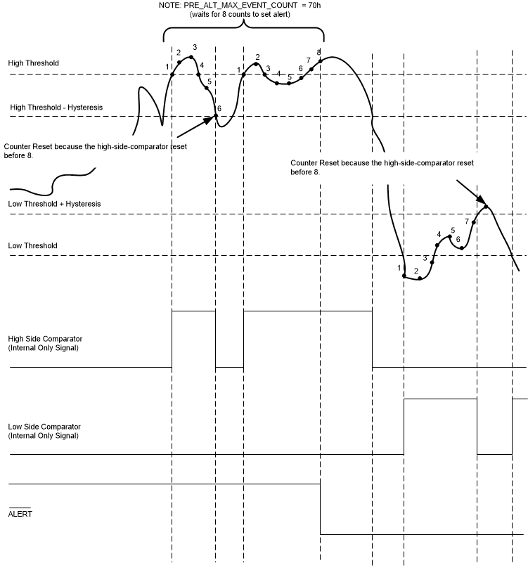
ADS7142 counter_alert_sbas773.gifFigure 48. Thresholds, Hysteresis and Event Counter for Digital Window Comparator

DWC_BLOCK_EN bit in ALERT_DWC_EN register enables/disables the complete Digital Window Comparator block (disabled at power-up) and ALERT_EN_CHx bits in ALERT_CHEN register enables Digital Window Comparator for individual channels. Once enabled, whenever a new conversion result is available:

  1. The output of the high side comparator transitions to logic high when the conversion result is greater than the High Threshold. This comparator resets when the conversion result is less than the High Threshold – Hysteresis.
  2. The output of the low side comparator transitions to logic high when the conversion result is less than the Low Threshold. This comparator resets when the conversion result is greater than the Low Threshold + Hysteresis.
  3. A different threshold and hysteresis can be used for each channel.
  4. Once the output of either the high side or low side comparator transitions high the Pre-Alert Event Counter begins to increment for each subsequent conversion. This counter continues to increment until it reaches the value stored in the PRE_ALT_MAX_EVENT_COUNT register. Once it reaches PRE_ALT_MAX_EVENT_COUNT, the Alert becomes active and sets the latched flags. If the comparator output becomes zero before counter reaches PRE_ALT_MAX_EVENT_COUNT, then the event counter is reset to zero, Alert does not be set and lateched flag is not set.

Therefore, the latched flags (high and low) for the channel are updated only if the respective comparator output remains 1 for the specified number of consecutive conversions (set by the PRE_ALT_MAX_EVENT_COUNT).

The latched flags can be read from the ALERT_LOW_FLAGS and ALERT_HIGH_FLAGS registers. To clear a latched flag, write 1 to the applicable bit location. The ALERT pin status is re-evaluated whenever an applicable latched flag gets set or is cleared.

The response time for ALERT pin can be estimated by Equation 6

Equation 6. tresponse = [1 + k x (PRE_ALT_MAX_EVENT_COUNT + 1) ] x nCLK x Oscillator TimePeriod

where

  • k is number of channels enabled in device sequence
  • nCLK is number of clocks used by device for one conversion cycle.
  • Oscillator Timer Period is tLPO or tHSO depending on OSC_SEL value . Refer to the Specifications for tLPO or tHSO .