ZHCSKI6T January 2006 – December 2023 TPS737
PRODUCTION DATA
- 1
- 1 特性
- 2 应用
- 3 说明
- 4 Pin Configuration and Functions
- 5 Specifications
- 6 Detailed Description
- 7 Application and Implementation
- 8 Device and Documentation Support
- 9 Revision History
- 10Mechanical, Packaging, and Orderable Information
封装选项
请参考 PDF 数据表获取器件具体的封装图。
机械数据 (封装 | 引脚)
- DCQ|6
- DRV|6
- DRB|8
散热焊盘机械数据 (封装 | 引脚)
订购信息
6.3.1 Output Noise
A precision band-gap reference is used to generate the internal reference voltage, Vref. This reference is the dominant noise source within the TPS737xx and generates approximately 32 μVRMS (10 Hz to 100 kHz) at the reference output (NR). The regulator control loop gains up the reference noise with the same gain as the reference voltage, so that the noise voltage of the regulator is approximately given by:
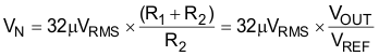
Because the value of VR is 1.2 V, this relationship reduces to:
for the case of no CNR.
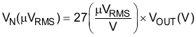
An internal 27-kΩ resistor in series with the noise-reduction pin (NR) forms a low-pass filter for the voltage reference when an external noise-reduction capacitor, CNR, is connected from NR to ground. For CNR = 10 nF, the total noise in the 10-Hz to 100-kHz bandwidth is reduced by a factor of approximately 3.2, giving the approximate relationship:
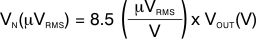
for CNR = 10 nF.
This noise reduction effect is shown as RMS Noise Voltage vs CNR in the Typical Characteristics section.
The TPS73701 adjustable version does not have the NR pin available. However, connecting a feedback capacitor, CFB, from the output to the feedback pin (FB) reduces output noise and improves load transient performance. Limit this capacitor to 0.1 µF.
The TPS737 uses an internal charge pump to develop an internal supply voltage sufficient to drive the gate of the NMOS pass transistor above VOUT. The charge pump generates approximately 250 μV of switching noise at approximately 4 MHz; however, charge-pump noise contribution is negligible at the output of the regulator for most values of IOUT and COUT.