ZHCSKI6T January   2006  – December 2023 TPS737

PRODUCTION DATA  

  1.   1
  2. 特性
  3. 应用
  4. 说明
  5. Pin Configuration and Functions
  6. Specifications
    1. 5.1 Absolute Maximum Ratings
    2. 5.2 ESD Ratings
    3. 5.3 Recommended Operating Conditions
    4. 5.4 Thermal Information
    5. 5.5 Electrical Characteristics
    6. 5.6 Typical Characteristics
  7. Detailed Description
    1. 6.1 Overview
    2. 6.2 Functional Block Diagrams
    3. 6.3 Feature Description
      1. 6.3.1 Output Noise
      2. 6.3.2 Internal Current Limit
      3. 6.3.3 Enable Pin and Shutdown
      4. 6.3.4 Reverse Current
    4. 6.4 Device Functional Modes
  8. Application and Implementation
    1. 7.1 Application Information
    2. 7.2 Typical Application
      1. 7.2.1 Design Requirements
      2. 7.2.2 Detailed Design Procedure
        1. 7.2.2.1 Input and Output Capacitor Requirements
        2. 7.2.2.2 Dropout Voltage
        3. 7.2.2.3 Transient Response
      3. 7.2.3 Application Curves
    3. 7.3 Best Design Practices
    4. 7.4 Power Supply Recommendations
    5. 7.5 Layout
      1. 7.5.1 Layout Guidelines
        1. 7.5.1.1 Power Dissipation
        2. 7.5.1.2 Thermal Protection
        3. 7.5.1.3 Estimating Junction Temperature
      2. 7.5.2 Layout Example
  9. Device and Documentation Support
    1. 8.1 Device Support
      1. 8.1.1 Development Support
        1. 8.1.1.1 Evaluation Modules
        2. 8.1.1.2 Spice Models
      2. 8.1.2 Device Nomenclature
    2. 8.2 Documentation Support
      1. 8.2.1 Related Documentation
    3. 8.3 接收文档更新通知
    4. 8.4 支持资源
    5. 8.5 Trademarks
    6. 8.6 静电放电警告
    7. 8.7 术语表
  10. Revision History
  11. 10Mechanical, Packaging, and Orderable Information

封装选项

请参考 PDF 数据表获取器件具体的封装图。

机械数据 (封装 | 引脚)
  • DCQ|6
  • DRV|6
  • DRB|8
散热焊盘机械数据 (封装 | 引脚)
订购信息

Transient Response

The low open-loop output impedance provided by the NMOS pass transistor in a voltage-follower configuration allows operation without a 1-µF output capacitor. As with any regulator, the addition of additional capacitance from the OUT pin to ground reduces undershoot magnitude but increases undershoot duration. In the adjustable version, the addition of a capacitor, CFB, from the OUT pin to the FB pin also improves the transient response.

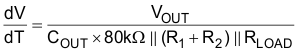
The TPS737 does not have an active pulldown when the output is overvoltage. This architecture allows applications that connect higher voltage sources, such as alternate power supplies, to the output. This architecture also results in an output overshoot of several percent if the load current quickly drops to zero when a capacitor is connected to the output. The duration of overshoot can be reduced by adding a load resistor. The overshoot decays at a rate determined by output capacitor COUT and the internal and external load resistance. The rate of decay is given by:

(Fixed voltage version)

Equation 4. GUID-54A23D33-FF6D-4BA5-9B8E-61478F512248-low.gif


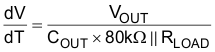
(Adjustable voltage version)

Equation 5. GUID-65DDF1AF-41E9-4670-9FAA-7005D3B2738A-low.gif