ZHCSCO8E June 2014 – May 2019 TPS65283 , TPS65283-1
PRODUCTION DATA.
- 1 特性
- 2 应用
- 3 说明
- 4 典型电路原理图
- 5 修订历史记录
- 6 说明 (续)
- 7 Pin Configuration and Functions
- 8 Specifications
-
9 Detailed Description
- 9.1 Overview
- 9.2 Functional Block Diagram
- 9.3
Feature Description
- 9.3.1 Power Switch Detailed Description
- 9.3.2
Buck DC-DC Converter Detailed Description
- 9.3.2.1 Output Voltage
- 9.3.2.2 Adjustable Switching Frequency
- 9.3.2.3 Synchronization
- 9.3.2.4 Error Amplifier
- 9.3.2.5 Slope Compensation
- 9.3.2.6 Enable and Adjusting UVLO
- 9.3.2.7 Internal V7V Regulator
- 9.3.2.8 Short Circuit Protection
- 9.3.2.9 Bootstrap Voltage (BST) and Low Dropout Operation
- 9.3.2.10 Output Overvoltage Protection (OVP)
- 9.3.2.11 Power Good
- 9.3.2.12 Power-Up Sequencing
- 9.3.2.13 Thermal Performance
- 9.4 Device Functional Modes
- 10Application and Implementation
- 11Power Supply Recommendations
- 12Layout
- 13器件和文档支持
- 14机械、封装和可订购信息
封装选项
机械数据 (封装 | 引脚)
- RGE|24
散热焊盘机械数据 (封装 | 引脚)
- RGE|24
订购信息
12.1.2 Power Dissipation and Junction Temperature
The total power dissipation inside TPS65283, TPS65283-1 should not to exceed the maximum allowable junction temperature of 125°C. The maximum allowable power dissipation is a function of the thermal resistance of the package (RθJA) and ambient temperature.
The following analysis gives an approximation in calculating junction temperature based on the power dissipation in the package. However, note that thermal analysis is strongly dependent on additional system-level factors. Such factors include air flow, board layout, copper thickness and surface area, and proximity to other devices dissipating power. Good thermal design practice must include all system-level factors in addition to individual component analysis.
To calculate the temperature inside the device under continuous load, use the following procedure.
- Define the total continuous current through buck converter (including the load current through power switches). Make sure the continuous current does not exceed maximum load current requirement.
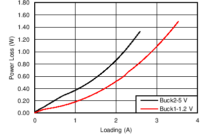
- From the graphs in this section, determine the expected losses (y-axis) in watts for buck converter inside the device. The loss PD_BUCK depends on the input supply and the selected switching frequency.
- Determine the load current IOUT through the power switches. Read RDS(on) of power switch from the typical characteristics graph.
- Calculate the power loss through power switches with PD_PW = RDS(on) × IOUT.
- The Thermal Information table provides the thermal resistance RθJA for specific packages and board layouts.
- To calculate the maximum temperature inside the IC, use Equation 21.
- TA = Ambient temperature (°C)
- RθJA = Thermal resistance (°C/W)
- PD_BUCK = Total power dissipation in buck converter (W)
- PD_PW = Total power dissipation in power switches (W)
where

