ZHCSCO8E June 2014 – May 2019 TPS65283 , TPS65283-1
PRODUCTION DATA.
- 1 特性
- 2 应用
- 3 说明
- 4 典型电路原理图
- 5 修订历史记录
- 6 说明 (续)
- 7 Pin Configuration and Functions
- 8 Specifications
-
9 Detailed Description
- 9.1 Overview
- 9.2 Functional Block Diagram
- 9.3
Feature Description
- 9.3.1 Power Switch Detailed Description
- 9.3.2
Buck DC-DC Converter Detailed Description
- 9.3.2.1 Output Voltage
- 9.3.2.2 Adjustable Switching Frequency
- 9.3.2.3 Synchronization
- 9.3.2.4 Error Amplifier
- 9.3.2.5 Slope Compensation
- 9.3.2.6 Enable and Adjusting UVLO
- 9.3.2.7 Internal V7V Regulator
- 9.3.2.8 Short Circuit Protection
- 9.3.2.9 Bootstrap Voltage (BST) and Low Dropout Operation
- 9.3.2.10 Output Overvoltage Protection (OVP)
- 9.3.2.11 Power Good
- 9.3.2.12 Power-Up Sequencing
- 9.3.2.13 Thermal Performance
- 9.4 Device Functional Modes
- 10Application and Implementation
- 11Power Supply Recommendations
- 12Layout
- 13器件和文档支持
- 14机械、封装和可订购信息
封装选项
机械数据 (封装 | 引脚)
- RGE|24
散热焊盘机械数据 (封装 | 引脚)
- RGE|24
订购信息
8.5 Electrical Characteristics
TJ = 25°C, VIN1 = VIN2 = 12 V, ƒSW = 500 kHz, RPG1 = RPG2 = RnFAULTx = 100 kΩ, unless otherwise noted| PARAMETER | TEST CONDITIONS | MIN | TYP | MAX | UNIT | |
|---|---|---|---|---|---|---|
| INPUT SUPPLY | ||||||
| VIN | Input voltage range | 4.5 | 18 | V | ||
| IDDSDN | Shutdown supply current | VSW_EN = VEN1 = VEN2 = 0 | 5.5 | 10 | µA | |
| IDDQ_NSW | None switching quiescent current | EN1 = EN2 = high, VFB1 = VFB2 = 1 V,
With buck1 and buck2 not switching |
0.5 | mA | ||
| UVLO | Input voltage undervoltage lockout (UVLO) | VIN1 rising | 4 | 4.25 | 4.5 | V |
| VIN1 falling | 3.5 | 3.75 | 4 | V | ||
| Hysteresis | 500 | mV | ||||
| V7V | Internal biasing supply | VV7V load current = 0 A, VIN1 = 12 V | 6.05 | 6.3 | 6.49 | V |
| IOCP_V7V | Current limit of V7V LDO | 180 | mA | |||
| OSCILLATOR | ||||||
| ƒSW | Switching frequency | ROSC = 100 kΩ | 400 | 500 | 600 | kHz |
| TSYNC_w | Clock sync minimum pulse width | 80 | ns | |||
| VSYNC_HI | Clock sync high threshold | 2 | V | |||
| VSYNC_LO | Clock sync low threshold | 0.4 | V | |||
| VSYNC_D | Clock falling edge to LX rising edge delay | 120 | ns | |||
| FSYNC | Clock sync frequency range | 200 | 2000 | kHz | ||
| BUCK1/BUCK2 CONVERTER | ||||||
| VFB | Feedback voltage | VCOMP1 = VCOMP2 = 1.2 V, TJ = 25°C | 0.594 | 0.6 | 0.606 | V |
| VCOMP1 = VCOMP2 = 1.2 V, TJ = –40°C to 125°C | 0.588 | 0.6 | 0.612 | V | ||
| Gm_EA | Error amplifier transconductance | –2 µA < ICOMPX < 2 µA | 300 | µS | ||
| Gm_SRC | COMP1/COMP2 voltage to inductor current Gm(1) | ILX1 = ILX2 = 0.5 A | 7.4 | A/V | ||
| VENXH | EN1, EN2 high level input voltage | 1.2 | 1.26 | V | ||
| VENXL | EN1, EN2 low-level input voltage | 1.1 | 1.15 | V | ||
| IENX | EN1, EN2 pullup current | VEN1 = VEN2 = 1 V | 3.6 | µA | ||
| IENX | EN1, EN2 pullup current | VEN1 = VEN2 = 1.5 V | 6.6 | µA | ||
| IENhys | IEN1 / IEN2 hysteresis current | 3 | µA | |||
| TON_MIN | Minimum on time | TJ = 25°C | 80 | 100 | ns | |
| TJ = –40°C to 125°C | 120 | |||||
| TSS_INT | Internal soft-start time | 2.4 | ms | |||
| ILIMIT1 | Buck1 peak inductor current limit | 4.25 | 5 | 5.75 | A | |
| ILIMITS1 | Buck1 low-side sink current limit | 1.7 | A | |||
| ILIMIT2 | Buck2 peak inductor current limit | 3.2 | 3.75 | 4.3 | A | |
| ILIMITS2 | Buck2 low side sink current limit | 1.3 | A | |||
| Rdson1_HS | High-side FET on-resistance in Buck1 | V7V = 6.25 V | 100 | mΩ | ||
| Rdson1_LS | Low-side FET on-resistance in buck1 | V7V = 6.25 V | 65 | mΩ | ||
| Rdson2_HS | High-side FET on-resistance in Buck2 | V7V = 6.25 V | 140 | mΩ | ||
| Rdson2_LS | Low-side FET on-resistance in buck2 | V7V = 6.25 V | 95 | mΩ | ||
| THICCUP_WAIT | Hiccup wait time | 4 | ms | |||
| THICCUP_RE | Hiccup time before restart | 64 | ms | |||
| POWER GOOD | ||||||
| Vth_PG | Feedback voltage threshold | VFB1 / VFB2 UV falling | 92.5% | |||
| VFB1 / VFB2 UV rising | 95% | |||||
| VFB1 / VFB2 OV rising | 107.5% | |||||
| VFB1 / VFB2 OV falling | 105% | |||||
| TDEGLITCH(PGF) | PG1/PG2 deglitch time (falling edge) | 1 | ms | |||
| TDEGLITCH(PGR) | PG1/PG2 deglitch time (rising edge) | 2 | ms | |||
| IPG | Power Good pin leakage | VFB1 = VFB2 = 0.6 V | 1 | µA | ||
| VLOW_PG | PG1/PG2 pin low voltage | Force FB1 = FB2 = 0.5 V, sink 1 mA to PG1/PG2 pin | 0.4 | V | ||
| POWER DISTRIBUTION SWITCH | ||||||
| VSWIN | Power switch input voltage range | 2.4 | 6 | V | ||
| IDDQH | Supply current, device enabled | No load on SW_OUT, RSET = 20 kΩ | 140 | µA | ||
| VUVLO_SW | Power switch input undervoltage lockout | VSWIN rising | 2.15 | 2.25 | 2.35 | V |
| VSWIN falling | 2.05 | 2.15 | 2.25 | V | ||
| Hysteresis | 100 | mV | ||||
| RDSON_SW | Power switch NMOS on-resistance | RGE package, VSWIN = 5 V, IOUT = 0.5 A,
TJ = 25°C, including bond wire resistance |
60 | mΩ | ||
| RGE package, VSWIN = 2.5 V, IOUT = 0.5 A,
TJ = 25°C, including bond wire resistance |
60 | mΩ | ||||
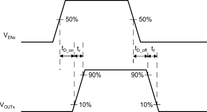
| tD_on | Turn-on delay time | VSWIN = 5 V, CL= 10 µF, RL= 100 Ω | 1.1 | ms | ||
| tD_off | Turn-off delay time | (See Figure 1) | 1.2 | ms | ||
| tr | Output rise time | 0.65 | ms | |||
| tf | Output fall time | 1.54 | ms | |||
| IOS | Current limit threshold (maximum DC current delivered to load) and short circuit current, OUT connect to ground | RSET = 14.3 kΩ | 1.575 | 1.75 | 1.925 | A |
| RSET = 20 kΩ | 1.125 | 1.25 | 1.375 | |||
| RSET = 50 kΩ | 0.4 | 0.5 | 0.6 | |||
| RSET = 80.6 kΩ, TJ = 0°C to 90°C | 0.15 | 0.325 | 0.5 | |||
| TDEGLITCH(OCP) | Switch overcurrent fault deglitch | Fault assertion or deassertion due to overcurrent condition | 6 | 8 | 10 | |
| ms | ||||||
| VL_nFAULT | nFAULT pin output low voltage | InFAULT = 1 mA | 150 | 300 | mV | |
| VENSWH | SW_EN high-level input voltage | 2 | V | |||
| VENSWL | SW_EN low-level input voltage | 0.4 | V | |||
| RDIS | Discharge resistance(2) | VSW_IN = 5 V, VSW_EN = 0 V | 100 | Ω | ||
| THERMAL SHUTDOWN | ||||||
| TTRIP_BUCK | Thermal protection trip point | Temperature rising | 160 | °C | ||
| THYST_BUCK | Hysteresis | 20 | ||||
| TTRIP_SW | Power switch thermal protection trip point
Power switch in overcurrent condition |
Temperature rise | 145 | °C | ||
| THYST_SW | Hysteresis | 20 | ||||
(1) Specified by design.
(2) The discharge function is active when the device is disabled (when enable is deasserted). The discharge function offers a resistive discharge path for the external storage capacitor.
 Figure 1. Power Switches Test Circuit and Voltage Waveforms
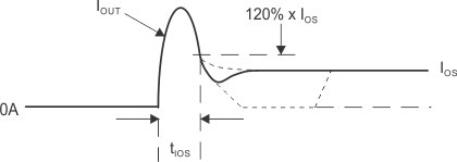
  Figure 2. Response Time to Short Circuit Waveform
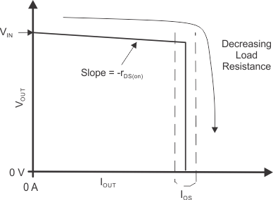
  Figure 3. Output Voltage vs Current Limit Threshold