ZHCSCO8E June   2014  – May 2019 TPS65283 , TPS65283-1

PRODUCTION DATA.  

  1. 特性
  2. 应用
  3. 说明
  4. 典型电路原理图
    1.     效率,Vin = 12V,PSM
  5. 修订历史记录
  6. 说明 (续)
  7. Pin Configuration and Functions
    1.     Pin Functions
  8. Specifications
    1. 8.1 Absolute Maximum Ratings
    2. 8.2 Handling Ratings
    3. 8.3 Recommended Operating Conditions
    4. 8.4 Thermal Information
    5. 8.5 Electrical Characteristics
    6. 8.6 Typical Characteristics
  9. Detailed Description
    1. 9.1 Overview
    2. 9.2 Functional Block Diagram
    3. 9.3 Feature Description
      1. 9.3.1 Power Switch Detailed Description
        1. 9.3.1.1 Overcurrent Condition
        2. 9.3.1.2 Reverse Current and Voltage Protection
        3. 9.3.1.3 nFAULT Response
        4. 9.3.1.4 UVLO
        5. 9.3.1.5 Enable and Output Discharge
        6. 9.3.1.6 Power Switch Input and Output Capacitance
        7. 9.3.1.7 Programming the Current-Limit Threshold
      2. 9.3.2 Buck DC-DC Converter Detailed Description
        1. 9.3.2.1  Output Voltage
        2. 9.3.2.2  Adjustable Switching Frequency
        3. 9.3.2.3  Synchronization
        4. 9.3.2.4  Error Amplifier
        5. 9.3.2.5  Slope Compensation
        6. 9.3.2.6  Enable and Adjusting UVLO
        7. 9.3.2.7  Internal V7V Regulator
        8. 9.3.2.8  Short Circuit Protection
          1. 9.3.2.8.1 High-Side MOSFET Overcurrent Protection
          2. 9.3.2.8.2 Low-Side MOSFET Overcurrent Protection
        9. 9.3.2.9  Bootstrap Voltage (BST) and Low Dropout Operation
        10. 9.3.2.10 Output Overvoltage Protection (OVP)
        11. 9.3.2.11 Power Good
        12. 9.3.2.12 Power-Up Sequencing
        13. 9.3.2.13 Thermal Performance
    4. 9.4 Device Functional Modes
      1. 9.4.1 Operation With VIN < 4.5 V (Minimum VIN)
      2. 9.4.2 Operation With EN Control
      3. 9.4.3 Operation at Light Loads
  10. 10Application and Implementation
    1. 10.1 Application Information
    2. 10.2 Typical Application
      1. 10.2.1 Design Requirements
      2. 10.2.2 Detailed Design Procedure
        1. 10.2.2.1 Output Voltage Setting
        2. 10.2.2.2 Bootstrap Capacitor Selection
        3. 10.2.2.3 Inductor Selection
        4. 10.2.2.4 Output Capacitor Selection
        5. 10.2.2.5 Input Capacitor Selection
        6. 10.2.2.6 Minimum Output Voltage
        7. 10.2.2.7 Compensation Component Selection
      3. 10.2.3 Application Curves
  11. 11Power Supply Recommendations
  12. 12Layout
    1. 12.1 Layout Guidelines
      1. 12.1.1 PCB Layout Recommendation
      2. 12.1.2 Power Dissipation and Junction Temperature
    2. 12.2 Layout Example
  13. 13器件和文档支持
    1. 13.1 文档支持
      1. 13.1.1 相关链接
    2. 13.2 商标
    3. 13.3 静电放电警告
    4. 13.4 Glossary
  14. 14机械、封装和可订购信息

封装选项

机械数据 (封装 | 引脚)
散热焊盘机械数据 (封装 | 引脚)
订购信息

Output Voltage

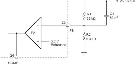
The TPS65283, TPS65283-1 regulate output voltage set by a feedback resistor divider to 0.6-V reference voltage. This pin should be directly connected to middle of resistor divider. TI recommends to use 1% tolerance or better divider resistors. Take care to route the FB line away from noise sources, such as the inductor or the LX switching node line. Start with 39 kΩ for the R1 resistor and use Equation 2 to calculate R2 and ensure the R2 ≤ 10 kΩ.

Equation 2. TPS65283 TPS65283-1 Eq02_R2_slvscl3.gif
TPS65283 TPS65283-1 buck_internal_feedback_resistor_divider_slvscl3.gifFigure 24. Buck Internal Feedback Resistor Divider