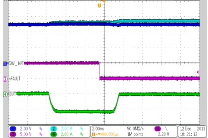
ZHCSCO8E June   2014  – May 2019 TPS65283 , TPS65283-1

PRODUCTION DATA.  

  1. 特性
  2. 应用
  3. 说明
  4. 典型电路原理图
    1.     效率,Vin = 12V,PSM
  5. 修订历史记录
  6. 说明 (续)
  7. Pin Configuration and Functions
    1.     Pin Functions
  8. Specifications
    1. 8.1 Absolute Maximum Ratings
    2. 8.2 Handling Ratings
    3. 8.3 Recommended Operating Conditions
    4. 8.4 Thermal Information
    5. 8.5 Electrical Characteristics
    6. 8.6 Typical Characteristics
  9. Detailed Description
    1. 9.1 Overview
    2. 9.2 Functional Block Diagram
    3. 9.3 Feature Description
      1. 9.3.1 Power Switch Detailed Description
        1. 9.3.1.1 Overcurrent Condition
        2. 9.3.1.2 Reverse Current and Voltage Protection
        3. 9.3.1.3 nFAULT Response
        4. 9.3.1.4 UVLO
        5. 9.3.1.5 Enable and Output Discharge
        6. 9.3.1.6 Power Switch Input and Output Capacitance
        7. 9.3.1.7 Programming the Current-Limit Threshold
      2. 9.3.2 Buck DC-DC Converter Detailed Description
        1. 9.3.2.1  Output Voltage
        2. 9.3.2.2  Adjustable Switching Frequency
        3. 9.3.2.3  Synchronization
        4. 9.3.2.4  Error Amplifier
        5. 9.3.2.5  Slope Compensation
        6. 9.3.2.6  Enable and Adjusting UVLO
        7. 9.3.2.7  Internal V7V Regulator
        8. 9.3.2.8  Short Circuit Protection
          1. 9.3.2.8.1 High-Side MOSFET Overcurrent Protection
          2. 9.3.2.8.2 Low-Side MOSFET Overcurrent Protection
        9. 9.3.2.9  Bootstrap Voltage (BST) and Low Dropout Operation
        10. 9.3.2.10 Output Overvoltage Protection (OVP)
        11. 9.3.2.11 Power Good
        12. 9.3.2.12 Power-Up Sequencing
        13. 9.3.2.13 Thermal Performance
    4. 9.4 Device Functional Modes
      1. 9.4.1 Operation With VIN < 4.5 V (Minimum VIN)
      2. 9.4.2 Operation With EN Control
      3. 9.4.3 Operation at Light Loads
  10. 10Application and Implementation
    1. 10.1 Application Information
    2. 10.2 Typical Application
      1. 10.2.1 Design Requirements
      2. 10.2.2 Detailed Design Procedure
        1. 10.2.2.1 Output Voltage Setting
        2. 10.2.2.2 Bootstrap Capacitor Selection
        3. 10.2.2.3 Inductor Selection
        4. 10.2.2.4 Output Capacitor Selection
        5. 10.2.2.5 Input Capacitor Selection
        6. 10.2.2.6 Minimum Output Voltage
        7. 10.2.2.7 Compensation Component Selection
      3. 10.2.3 Application Curves
  11. 11Power Supply Recommendations
  12. 12Layout
    1. 12.1 Layout Guidelines
      1. 12.1.1 PCB Layout Recommendation
      2. 12.1.2 Power Dissipation and Junction Temperature
    2. 12.2 Layout Example
  13. 13器件和文档支持
    1. 13.1 文档支持
      1. 13.1.1 相关链接
    2. 13.2 商标
    3. 13.3 静电放电警告
    4. 13.4 Glossary
  14. 14机械、封装和可订购信息

封装选项

机械数据 (封装 | 引脚)
散热焊盘机械数据 (封装 | 引脚)
订购信息

Application Curves

TJ = 25°C, Vin = 12 V, Vout1 = 1.2 V, Vout2 = 5 V, ƒSW = 500 kHz, RnFAULT1 = RnFAULT2 = 100 kΩ (unless otherwise noted)
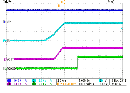
TPS65283 TPS65283-1 osc_01_LVSCL3.gifFigure 32. Buck1 Start Up by EN1 Pin With 2-A Loading
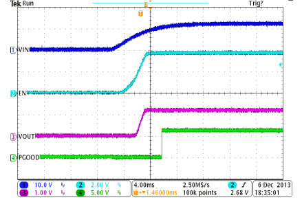
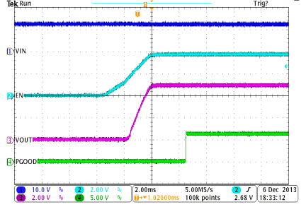
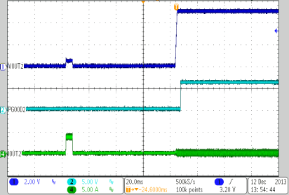
TPS65283 TPS65283-1 osc_03_LVSCL3.gifFigure 34. Ramp Vin to Start Up Buck1 With 2-A Loading
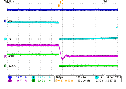
TPS65283 TPS65283-1 osc_05_LVSCL3.gifFigure 36. Buck1 Shut Down by EN1 Pin With 2-A Loading
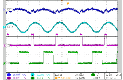
TPS65283 TPS65283-1 osc_07_LVSCL3.gif
Iout1 = Iout2 = 0 A
Figure 38. Buck Output Voltage Ripple in PWM Mode
TPS65283 TPS65283-1 osc_09_LVSCL3.gif
Iout1 = Iout2 = 0.1 A
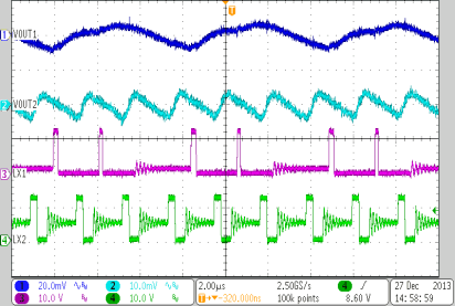
Figure 40. Buck Output Voltage Ripple in PSM Mode
TPS65283 TPS65283-1 osc_11_LVSCL3.gif
Iout1 = Iout2 = 0 to 1 A
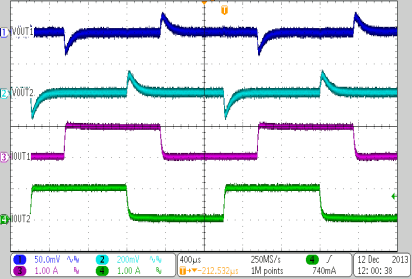
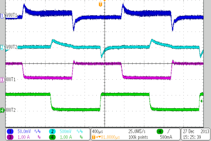
Figure 42. Buck Output Load Transient in PWM Mode
TPS65283 TPS65283-1 osc_13_LVSCL3.gif
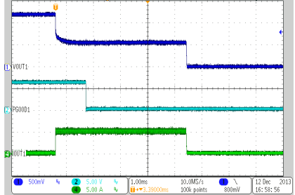
Figure 44. Buck1 Response to Hard Short
TPS65283 TPS65283-1 osc_15_LVSCL3.gif
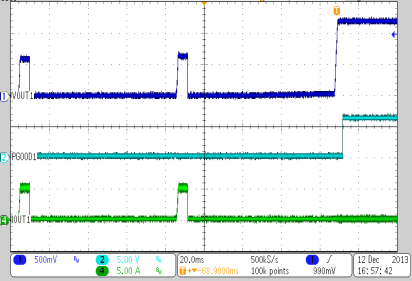
Figure 46. Buck1 Recovery from Hiccup
TPS65283 TPS65283-1 osc_17_LVSCL3.gif
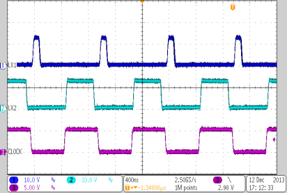
Figure 48. Clock Synchronization at 1 MHz
TPS65283 TPS65283-1 osc_19_LVSCL3.gif
Rout = 50 Ω, Cout = 10 μF
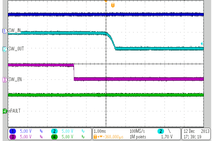
Figure 50. Power Switch Turn off Delay and Fall Time
TPS65283 TPS65283-1 osc_21_LVSCL3.gif
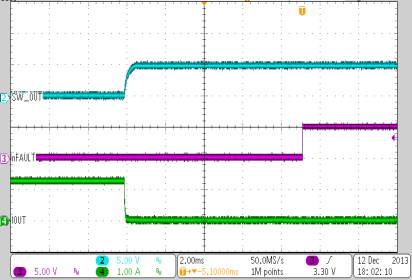
Figure 52. Power Switch Recovery from Over-Current
TPS65283 TPS65283-1 osc_23_LVSCL3.gif
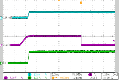
Figure 54. Power Switch Enable into Short Circuit
TPS65283 TPS65283-1 osc_02_LVSCL3.gifFigure 33. Buck2 Start Up by EN2 Pin With 2-A Loading
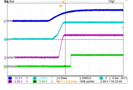
TPS65283 TPS65283-1 osc_04_LVSCL3.gifFigure 35. Ramp Vin to Start Up Buck2 With 2-A Loading
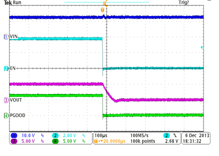
TPS65283 TPS65283-1 osc_06_LVSCL3.gifFigure 37. Buck2 Shut Down by EN2 Pin With 2-A Loading
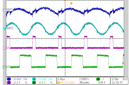
TPS65283 TPS65283-1 osc_08_LVSCL3.gif
Iout1 = Iout2 = 2.5 A
Figure 39. Buck Output Voltage Ripple in PWM Mode
TPS65283 TPS65283-1 osc_10_LVSCL3.gif
Iout1 = Iout2 = 0 to 1 A
Figure 41. Buck Output Load Transient in PSM Mode
TPS65283 TPS65283-1 osc_12_LVSCL3.gif
Iout1 = 2.5 to 3.5 A, Iout2 = 1.5 to 2.5 A
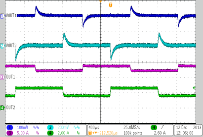
Figure 43. Buck Output Load Transient in PWM Mode
TPS65283 TPS65283-1 osc_14_LVSCL3.gif
Figure 45. Buck2 Response to Hard Short
TPS65283 TPS65283-1 osc_16_LVSCL3.gif
Figure 47. Buck2 Recovery from Hiccup
TPS65283 TPS65283-1 osc_18_LVSCL3.gif
Rout = 50 Ω, Cout = 10 μF
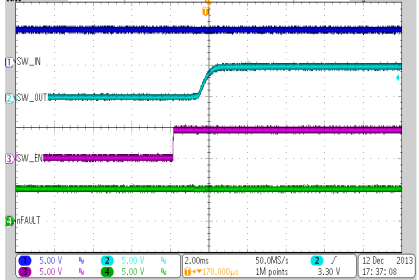
Figure 49. Power Switch Turn on Delay and Rising Time
TPS65283 TPS65283-1 osc_20_LVSCL3.gif
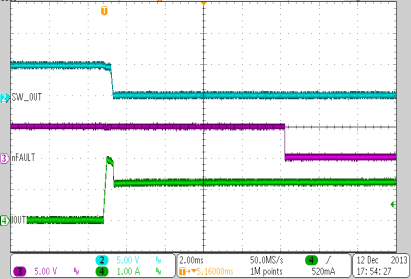
Figure 51. Power Switch Over Current With 2-A Loading
TPS65283 TPS65283-1 osc_22_LVSCL3.gif
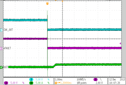
Figure 53. Power Switch Hard Short Operation
TPS65283 TPS65283-1 osc_24_LVSCL3.gif
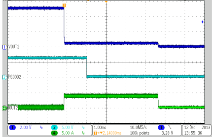
Figure 55. Power Switch Reverse Voltage Protection Response