ZHCSCL5D january 2014 – may 2023 TPS65262
PRODUCTION DATA
- 1
- 1 特性
- 2 应用
- 3 说明
- 4 Revision History
- 5 Pin Configuration and Functions
- 6 Specifications
-
7 Detailed Description
- 7.1 Overview
- 7.2 Functional Block Diagram
- 7.3
Feature Description
- 7.3.1 Adjusting the Output Voltage
- 7.3.2 Enable and Adjusting Undervoltage Lockout
- 7.3.3 Soft-Start Time
- 7.3.4 Power-Up Sequencing
- 7.3.5 V7V Low Dropout Regulator and Bootstrap
- 7.3.6 Out-of-Phase Operation
- 7.3.7 Output Overvoltage Protection (OVP)
- 7.3.8 PSM
- 7.3.9 Slope Compensation
- 7.3.10 Overcurrent Protection
- 7.3.11 Power Good
- 7.3.12 Thermal Shutdown
- 7.4 Device Functional Modes
- 8 Application and Implementation
- 9 Device and Documentation Support
- 10Mechanical, Packaging, and Orderable Information
7.3.1 Adjusting the Output Voltage
The output voltage of each buck is set with a resistor divider from the output of buck to the FB pin. TI recommends to use 1% tolerance or better divider resistors.
 Figure 7-1 Voltage Divider Circuit
Equation 1. 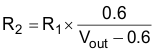
To improve efficiency at light loads consider using larger value resistors. If the values are too high, the regulator is more sensitive to noise. The recommended resistor values are shown in Table 7-1.
Table 7-1 Output Resistor Divider Selection
| OUTPUT VOLTAGE (V) | R1 (kΩ) | R2 (kΩ) |
|---|---|---|
| 1 | 10 | 15 |
| 1.2 | 10 | 10 |
| 1.5 | 15 | 10 |
| 1.8 | 20 | 10 |
| 2.5 | 31.6 | 10 |
| 3.3 | 45.3 | 10 |
| 3.3 | 22.6 | 4.99 |
| 5 | 73.2 | 10 |
| 5 | 36.5 | 4.99 |