ZHCSCL5D january 2014 – may 2023 TPS65262
PRODUCTION DATA
- 1
- 1 特性
- 2 应用
- 3 说明
- 4 Revision History
- 5 Pin Configuration and Functions
- 6 Specifications
-
7 Detailed Description
- 7.1 Overview
- 7.2 Functional Block Diagram
- 7.3
Feature Description
- 7.3.1 Adjusting the Output Voltage
- 7.3.2 Enable and Adjusting Undervoltage Lockout
- 7.3.3 Soft-Start Time
- 7.3.4 Power-Up Sequencing
- 7.3.5 V7V Low Dropout Regulator and Bootstrap
- 7.3.6 Out-of-Phase Operation
- 7.3.7 Output Overvoltage Protection (OVP)
- 7.3.8 PSM
- 7.3.9 Slope Compensation
- 7.3.10 Overcurrent Protection
- 7.3.11 Power Good
- 7.3.12 Thermal Shutdown
- 7.4 Device Functional Modes
- 8 Application and Implementation
- 9 Device and Documentation Support
- 10Mechanical, Packaging, and Orderable Information
8.2.3 Application Curves
TA = 25°C, VIN = 12 V, VOUT1 = 1.2 V, VOUT2 = 1.8 V, VOUT3 =
3.3 V, ƒSW = 600 kHz (unless otherwise noted)
TA = 25°C, VIN = 12 V, VOUT1 = 1.2 V, VOUT2 = 1.8 V, VOUT3 =
3.3 V, ƒSW = 600 kHz (unless otherwise noted)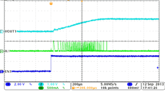 Figure 8-3 Buck1, Soft-Start With No Load. TA = 25°C, VIN = 12 V, VOUT1 = 1.2 V, VOUT2 = 1.8 V, VOUT3 =
3.3 V, ƒSW = 600 kHz (unless otherwise noted)
 Figure 8-3 Buck1, Soft-Start With No Load. TA = 25°C, VIN = 12 V, VOUT1 = 1.2 V, VOUT2 = 1.8 V, VOUT3 =
3.3 V, ƒSW = 600 kHz (unless otherwise noted)
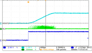 Figure 8-5 Buck2, Soft-Start With No Load
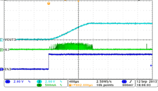 Figure 8-7 Buck3, Soft-Start With No Load
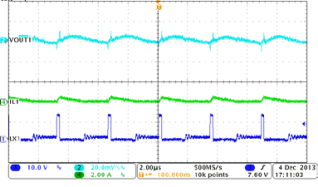 Figure 8-9 Buck1, Steady State Operation With Light Load
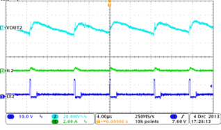 Figure 8-11 Buck2, Steady State Operation With Light Load
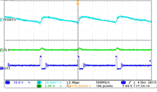 Figure 8-13 Buck3, Steady State Operation With Light Load
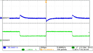 Figure 8-15 Buck1, Load Transient, 0.75 to 1.5 A SR = 0.25 A/µs
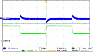 Figure 8-17 Buck2, Load Transient, 0.25 to 0.5 A SR = 0.25 A/µs
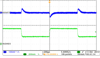 Figure 8-19 Buck3, Load Transient, 0.25 to 0.5 A SR = 0.25 A/µs
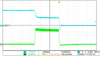 Figure 8-21 Buck1, Overcurrent Protection
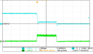 Figure 8-23 Buck2, Overcurrent Protection
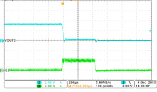 Figure 8-25 Buck3, Overcurrent Protection
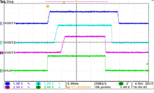 Figure 8-27 Automatic Power Sequencing, MODE = EN1 = EN2 = HIGH
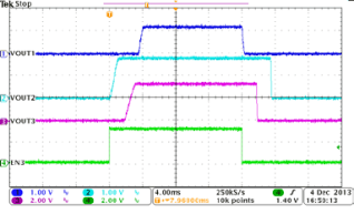 Figure 8-29 Automatic Power Sequencing, MODE = EN1 = HIGH, EN2 = LOW
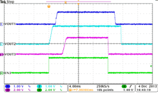 Figure 8-31 Automatic Power Sequencing, MODE = EN2 = HIGH, EN1 = LOW
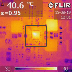
| Operating at VIN = 12 V | VOUT1 = 1.2 V/1.5 A | |
| VOUT3 = 3.3 V/0.5 A | VOUT2 = 1.8 V/0.5 A |
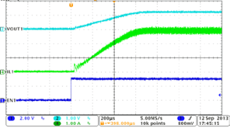 Figure 8-4 Buck1, Soft-Start With Full Load
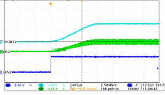 Figure 8-6 Buck2, Soft-Start With Full Load
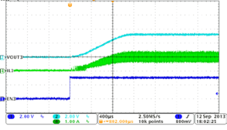 Figure 8-8 Buck3, Soft-Start With Full Load
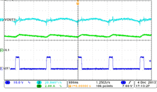 Figure 8-10 Buck1, Steady State Operation With Full Load
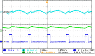 Figure 8-12 Buck2, Steady State Operation With Full Load
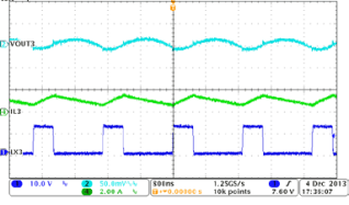 Figure 8-14 Buck3, Steady State Operation With Full Load
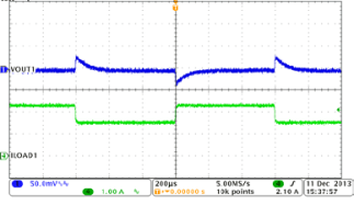 Figure 8-16 Buck1, Load Transient, 1.5 to 2.25 A SR = 0.25 A/µs
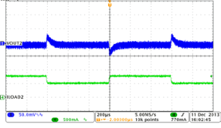 Figure 8-18 Buck2, Load Transient, 0.5 to 0.75 A SR = 0.25A/µs
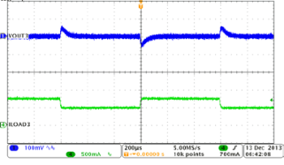 Figure 8-20 Buck3, Load Transient, 0.5 to 0.75 A SR = 0.25A/µs
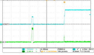 Figure 8-22 Buck1, Hiccup and Recovery
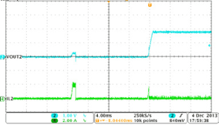 Figure 8-24 Buck2, Hiccup and Recovery
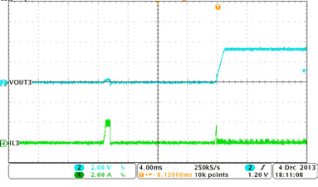 Figure 8-26 Buck3, Hiccup and Recovery
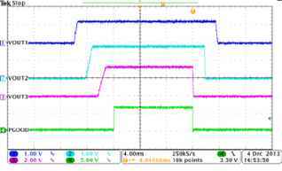 Figure 8-28 Automatic Power Sequencing, MODE = EN1 = EN2 = HIGH
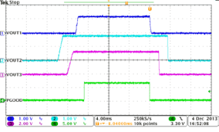 Figure 8-30 Automatic Power Sequencing, MODE = EN1 = HIGH, EN2 = LOW
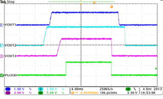 Figure 8-32 Automatic Power Sequencing, MODE = EN2 = HIGH, EN1 = LOW
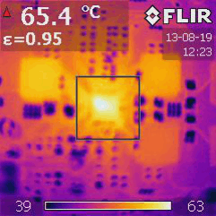
| Operating at VIN = 12 V | VOUT1 = 1.2 V/3 A | |
| VOUT3 = 3.3 V/1 A | VOUT2 = 1.8 V/1 A |