TA = 25°C, VIN = 12 V, fSW = 1 MHz, CBoost = (2 × 22 µF / 35 V) (unless otherwise noted)
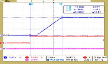
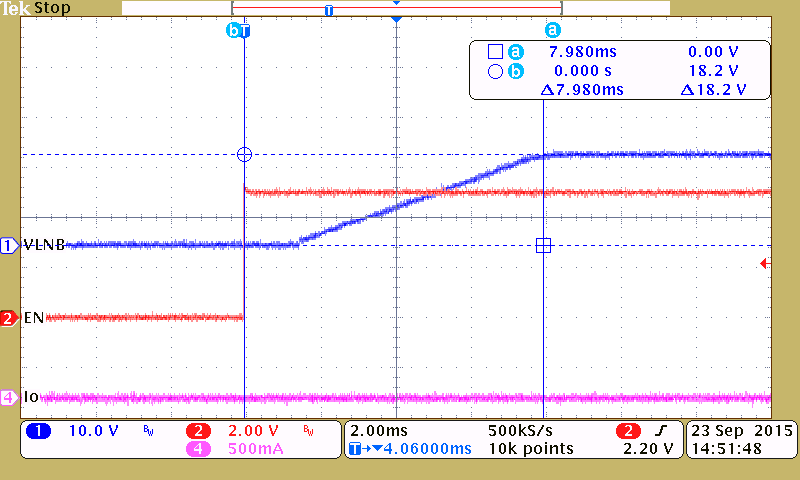
 Figure 8-2 Soft Start, Delay from EN High to LNB Output High
 Figure 8-4 Soft-Start, Delay from EN High to LNB Output High
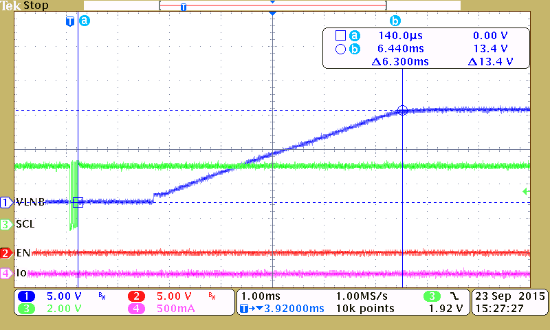
 Figure 8-6 Soft Start, Delay From I2C Enable (I2C_CON = 1b) to LNB Output High
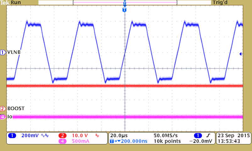
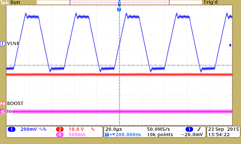
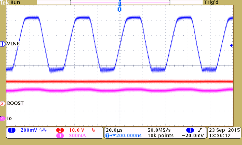
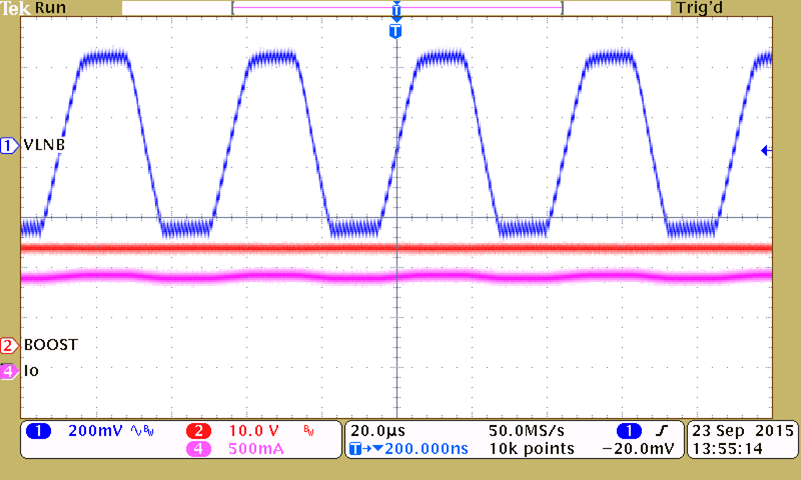
 Figure 8-8 No Load, 22-kHz Tone Output
 Figure 8-10 No Load, 22-kHz Tone Output
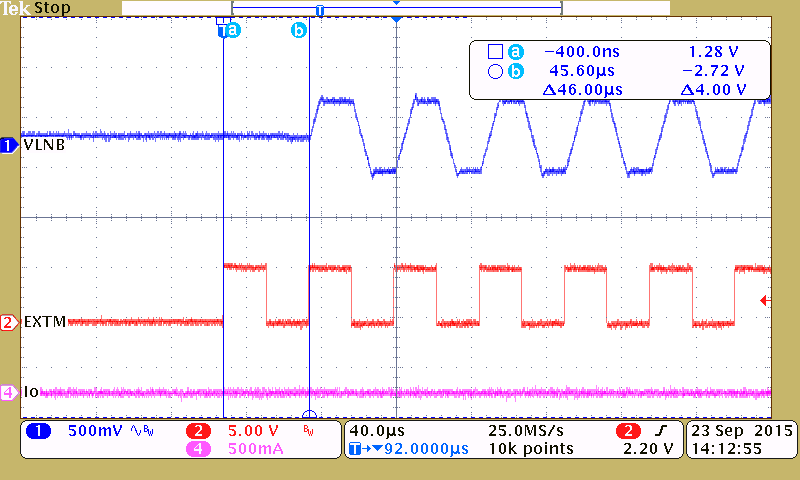
 Figure 8-12 No load, 22-kHz Tone Delay from EXTM 22-kHz Input Turns High to Output Tone On
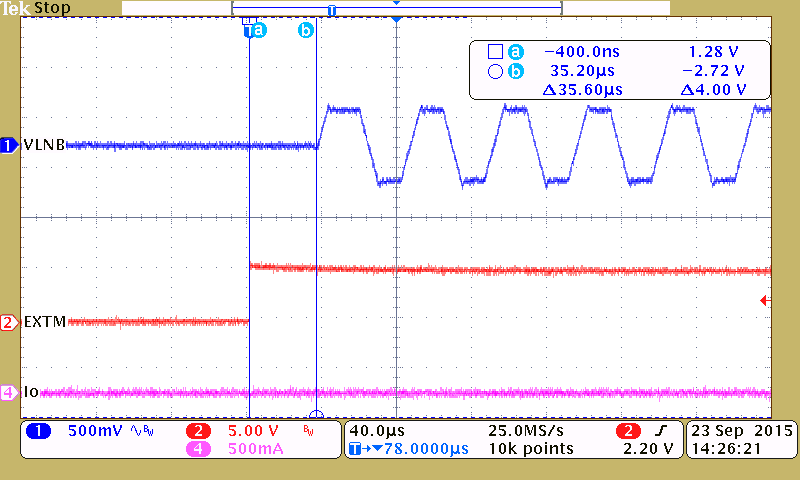
 Figure 8-14 No Load, 22-kHz Tone Delay from EXTM Tone Envelop Input Turns High to Output Tone On
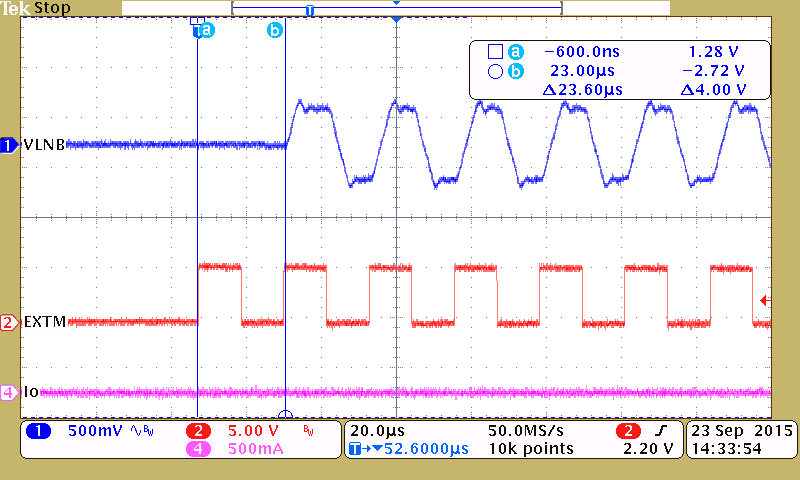
 Figure 8-16 No Load, 44-kHz Tone Delay from EXTM 22-kHz Input Turns High to Output Tone On
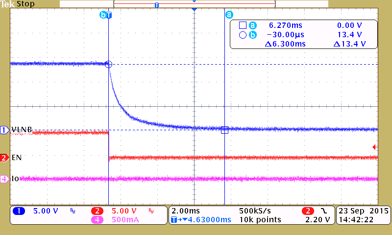
 Figure 8-3 Disabled, Delay from EN Low to LNB Output Low
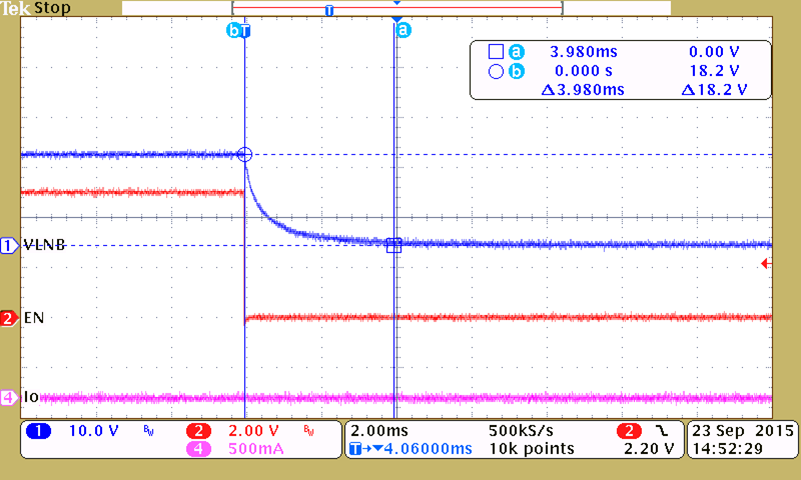
 Figure 8-5 Disabled, Delay From EN Low to LNB Output Low
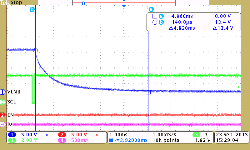
 Figure 8-7 Delay From I2C Disable (I2C_CON = 0b) to LNB Output Low
 Figure 8-9 950-mA Load, 22-kHz Tone Output
 Figure 8-11 950-mA Load, 22-kHz Tone Output
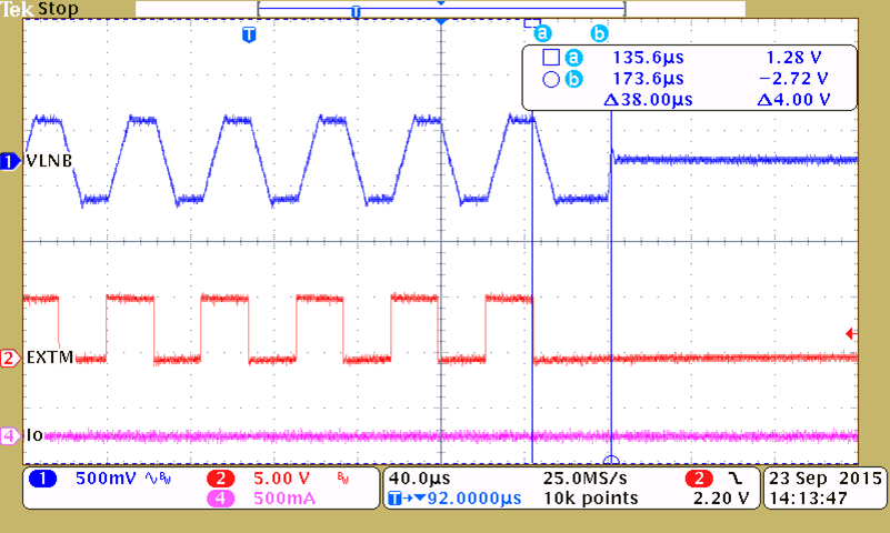
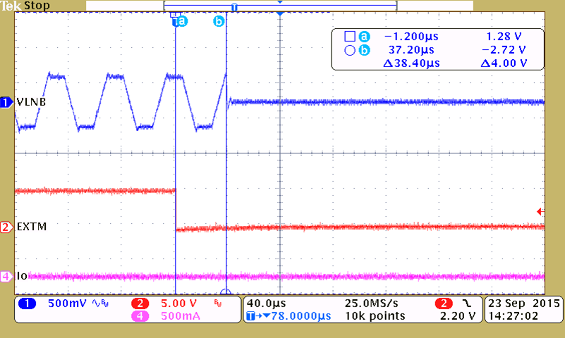
 Figure 8-13 No load, 22-kHz Tone Delay from EXTM 22-kHz Input Turns Low to Output Tone Off
 Figure 8-15 No Load, 22-kHz Tone Delay from EXTM Tone Envelop Input Turns Low to Output Tone Off
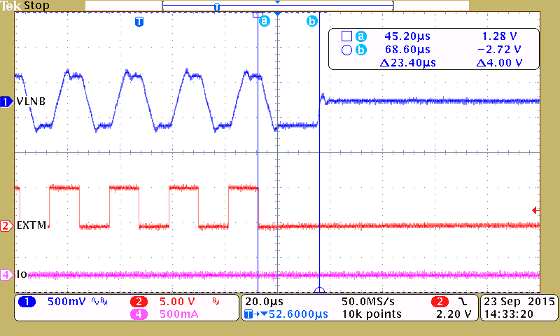
 Figure 8-17 No Load, 44-kHz Tone Delay from EXTM 22-kHz Input Turns Low to Output Tone Off