ZHCSGR8A September   2017  – July 2018 TPS63710

PRODUCTION DATA.  

  1. 特性
  2. 应用
  3. 说明
    1.     Device Images
      1.      典型应用
      2.      VOUT = -1.8V 时效率与输出电流间的关系
  4. 修订历史记录
  5. Pin Configuration and Functions
    1. Table 1. Pin Functions
  6. Specifications
    1. 6.1 Absolute Maximum Ratings
    2. 6.2 ESD Ratings
    3. 6.3 Recommended Operating Conditions
    4. 6.4 Thermal Information
    5. 6.5 Electrical Characteristics
    6. 6.6 Typical Characteristics
  7. Detailed Description
    1. 7.1 Overview
    2. 7.2 Functional Block Diagram
    3. 7.3 Feature Description
      1. 7.3.1 Low Noise Reference System
      2. 7.3.2 Duty Cycle
      3. 7.3.3 Enable
      4. 7.3.4 Undervoltage Lockout
      5. 7.3.5 Thermal Shutdown
      6. 7.3.6 Power Good Output
    4. 7.4 Device Functional Modes
      1. 7.4.1 Soft-Start
      2. 7.4.2 VOUT Discharge
      3. 7.4.3 Current Limit
      4. 7.4.4 CCP Capacitor Precharge
      5. 7.4.5 PWM Operation
  8. Application and Implementation
    1. 8.1 Application Information
    2. 8.2 Typical Application
      1. 8.2.1 Design Requirements
      2. 8.2.2 Detailed Design Procedure
        1. 8.2.2.1 Custom Design With WEBENCH® Tools
        2. 8.2.2.2 Setting the Output Voltage
        3. 8.2.2.3 Inductor Selection
        4. 8.2.2.4 Capacitor Selection
          1. 8.2.2.4.1 CCP Capacitor
          2. 8.2.2.4.2 Input Capacitor
          3. 8.2.2.4.3 Output Capacitor
      3. 8.2.3 Application Curves
        1. 8.2.3.1 Parameter Measurement Information
    3. 8.3 System Examples
      1. 8.3.1 Typical Application for Powering the Negative Rail of a Gallium Nitride (GaN) Power Amplifier
      2. 8.3.2 Typical Application for Powering the Negative Rail of an ADC or DAC
      3. 8.3.3 Typical Application for Laser Diode Bias
  9. Power Supply Recommendations
  10. 10Layout
    1. 10.1 Layout Guidelines
    2. 10.2 Layout Example
  11. 11器件和文档支持
    1. 11.1 器件支持
      1. 11.1.1 使用 WEBENCH® 工具创建定制设计
      2. 11.1.2 第三方产品免责声明
    2. 11.2 社区资源
    3. 11.3 商标
    4. 11.4 静电放电警告
    5. 11.5 术语表
  12. 12机械、封装和可订购信息

封装选项

机械数据 (封装 | 引脚)
散热焊盘机械数据 (封装 | 引脚)
订购信息

Typical Application

The application covers the input voltage range from 4.5 V to 14 V at the full 1-A output current. The output capacitors are designed for an output voltage of -1.8 V. With output voltages below -1.8V (larger negative voltages), the output capacitance has to be increased as described in the Detailed Design Procedure. The minimum supply voltage is defined by the 70% duty cycle limit, output current and the output voltage. Please see Figure 36 to Figure 38 for the recommended input voltage levels to generate a specific output voltage.
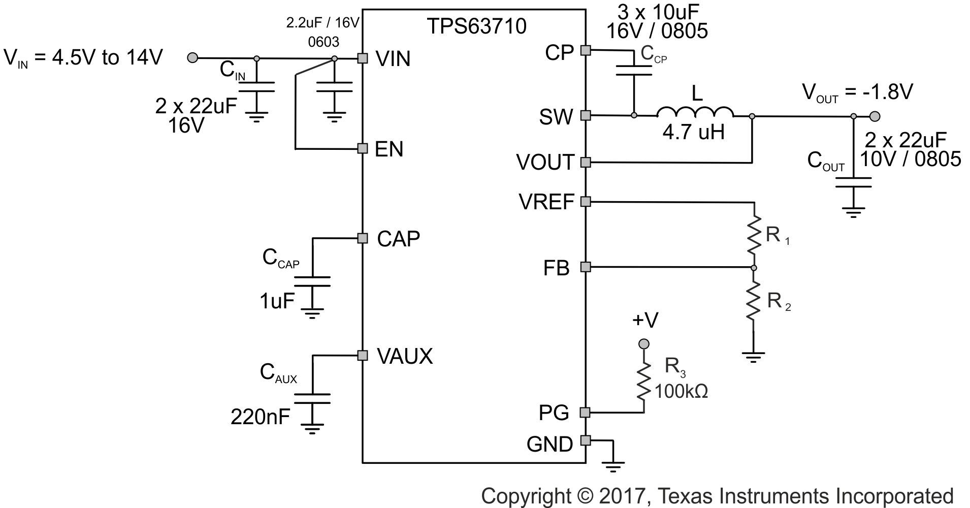
TPS63710 TPS63710_1V8application_fullVIN.gifFigure 9. Typical Application for an Input Voltage up to 14V