ZHCSHG3B november   2017  – july 2020 TPS254900A-Q1

PRODUCTION DATA  

  1.   1
  2. 特性
  3. 应用
  4. 说明
  5. Revision History
  6. Pin Configuration and Functions
    1.     7
  7. Specifications
    1. 6.1 Absolute Maximum Ratings
    2. 6.2 ESD Ratings
    3. 6.3 Recommended Operating Conditions
    4. 6.4 Thermal Information
    5. 6.5 Electrical Characteristics
    6. 6.6 Switching Characteristics
    7. 6.7 Typical Characteristics
  8. Parameter Measurement Information
  9. Detailed Description
    1. 8.1 Overview
    2. 8.2 Functional Block Diagram
    3. 8.3 Feature Description
      1. 8.3.1  FAULT Response
      2. 8.3.2  Cable Compensation
        1. 8.3.2.1 Design Procedure
      3. 8.3.3  D+ and D– Protection
      4. 8.3.4  VBUS OVP Protection
      5. 8.3.5  Output and D+ or D– Discharge
      6. 8.3.6  Port Power Management (PPM)
        1. 8.3.6.1 Benefits of PPM
        2. 8.3.6.2 PPM Details
        3. 8.3.6.3 Implementing PPM in a System With Two Charging Ports (CDP and SDP1)
      7. 8.3.7  Overcurrent Protection
      8. 8.3.8  Undervoltage Lockout
      9. 8.3.9  Thermal Sensing
      10. 8.3.10 Current-Limit Setting
    4. 8.4 Device Functional Modes
      1. 8.4.1 Device Truth Table (TT)
      2. 8.4.2 USB BC1.2 Specification Overview
      3. 8.4.3 Standard Downstream Port (SDP) Mode — USB 2.0 and USB 3.0
      4. 8.4.4 Charging Downstream Port (CDP) Mode
      5. 8.4.5 Client Mode
      6. 8.4.6 High-Bandwidth Data-Line Switch
  10. Application and Implementation
    1. 9.1 Application Information
    2. 9.2 Typical Application
      1. 9.2.1 Design Requirements
      2. 9.2.2 Detailed Design Procedure
        1. 9.2.2.1 Input Capacitance
        2. 9.2.2.2 Output Capacitance
        3. 9.2.2.3 BIAS Capacitance
        4. 9.2.2.4 Output and BIAS TVS
      3. 9.2.3 Application Curves
  11. 10Power Supply Recommendations
  12. 11Layout
    1. 11.1 Layout Guidelines
    2. 11.2 Layout Example
  13. 12Device and Documentation Support
    1. 12.1 Device Support
    2. 12.2 Documentation Support
      1. 12.2.1 Related Documentation
    3. 12.3 接收文档更新通知
    4. 12.4 支持资源
    5. 12.5 Trademarks
    6. 12.6 静电放电警告
    7. 12.7 术语表
  14. 13Mechanical, Packaging, and Orderable Information

封装选项

请参考 PDF 数据表获取器件具体的封装图。

机械数据 (封装 | 引脚)
  • RVC|20
散热焊盘机械数据 (封装 | 引脚)
订购信息

Cable Compensation

When a load draws current through a long or thin wire, there is an IR drop that reduces the voltage delivered to the load. In the vehicle from the voltage regulator 5-V output to the VPD_IN (input voltage of portable device), the total resistance of power switch rDS(on) and cable resistance causes an IR drop at the PD input. So the charging current of most portable devices is less than their expected maximum charging current.
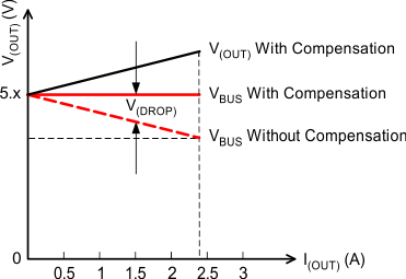
GUID-0327A98B-3157-4629-9115-D36AA63DC162-low.gifFigure 8-1 Voltage Drop

The TPS254900A-Q1 device detects the load current and applies a proportional sink current that can be used to adjust the output voltage of the upstream regulator to compensate for the IR drop in the charging path. The gain G(CS) of the sink current proportional to load current is 82 µA/A.
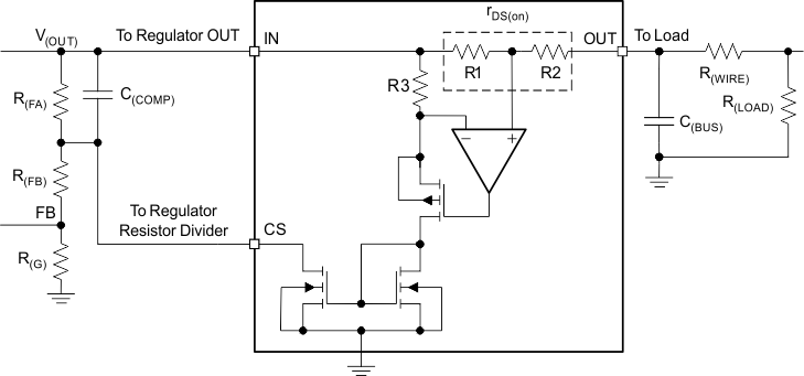
GUID-E3B7EEF0-6EEC-460E-9C85-2621FBB1A1D4-low.gifFigure 8-2 Cable Compensation Equivalent Circuit