ZHCSHG3B november 2017 – july 2020 TPS254900A-Q1
PRODUCTION DATA
- 1
- 1 特性
- 2 应用
- 3 说明
- 4 Revision History
- 5 Pin Configuration and Functions
- 6 Specifications
- 7 Parameter Measurement Information
-
8 Detailed Description
- 8.1 Overview
- 8.2 Functional Block Diagram
- 8.3 Feature Description
- 8.4 Device Functional Modes
- 9 Application and Implementation
- 10Power Supply Recommendations
- 11Layout
- 12Device and Documentation Support
- 13Mechanical, Packaging, and Orderable Information
封装选项
请参考 PDF 数据表获取器件具体的封装图。
机械数据 (封装 | 引脚)
- RVC|20
散热焊盘机械数据 (封装 | 引脚)
- RVC|20
订购信息
8.3.10 Current-Limit Setting
The TPS254900A-Q1 has two independent current-limit settings that are each adjusted externally with a resistor. The ILIM_HI setting is adjusted with R(ILIM_HI) connected between ILIM_HI and GND. The ILIM_LO setting is adjusted with R(ILIM_LO) connected between ILIM_LO and GND. Consult the device truth table (Table 8-3) to see when each current limit is used. Both settings have the same relation between the current limit and the adjusting resistor.
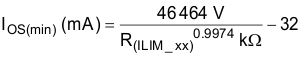
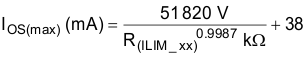
The following equation calculates the value of resistor for adjusting the typical current limit:
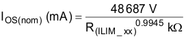
Many applications require that the current limit meet specific tolerance limits. When designing to these tolerance limits, both the tolerance of the TPS254900A-Q1 current limit and the tolerance of the external adjusting resistor must be taken into account. The following equations approximate the TPS254900A-Q1 minimum and maximum current limits to within a few milliamperes and are appropriate for design purposes. The equations do not constitute part of TI’s published device specifications for purposes of TI’s product warranty. These equations assume an ideal—no variation—external adjusting resistor. To take resistor tolerance into account, first determine the minimum and maximum resistor values based on its tolerance specifications and use these values in the equations. Because of the inverse relation between the current limit and the adjusting resistor, use the maximum resistor value in the IOS(min) equation and the minimum resistor value in the IOS(max) equation.


The routing of the traces to the R(ILIM_xx) resistors should have a sufficiently low resistance so as not to affect the current-limit accuracy. The ground connection for the R(ILIM_xx) resistors is also very important. The resistors must reference back to the TPS254900A-Q1 GND pin. Follow normal board layout practices to ensure that current flow from other parts of the board does not impact the ground potential between the resistors and the TPS254900A-Q1 GND pin.