ZHCSG62A March 2017 – May 2017 TPD2S703-Q1
PRODUCTION DATA.
- 1 特性
- 2 应用
- 3 说明
- 4 修订历史记录
- 5 Pin Configuration and Functions
-
6 Specifications
- 6.1 Absolute Maximum Ratings
- 6.2 ESD Ratings—AEC Specification
- 6.3 ESD Ratings—IEC Specification
- 6.4 ESD Ratings—ISO Specification
- 6.5 Recommended Operating Conditions
- 6.6 Thermal Information
- 6.7 Electrical Characteristics
- 6.8 Power Supply and Supply Current Consumption Chracteristics
- 6.9 Timing Requirements
- 6.10 Typical Characteristics
- 7 Parameter Measurement Information
- 8 Detailed Description
- 9 Application and Implementation
- 10Power Supply Recommendations
- 11Layout
- 12器件和文档支持
- 13机械、封装和可订购信息
封装选项
机械数据 (封装 | 引脚)
散热焊盘机械数据 (封装 | 引脚)
- DSK|10
订购信息
6.9 Timing Requirements
over operating free-air temperature range (unless otherwise noted)| MIN | NOM | MAX | UNIT | |||
|---|---|---|---|---|---|---|
| ENABLE PIN AND VREF FAST CHARGE | ||||||
| TVREF_CHG | VREF fast charge time | Time between when 5 V is applied to VPWR, and VREF reaches VVREF_FAST_CHG. Needs to happen before or at same time tON_STARTUP completes | 0.5 | 1 | ms | |
| TON_STARTUP_MODE0 | Device turnon time from UVLO mode 0 | Mode 0. EN = 0 V, measured from VPWR and VREF = UVLO+ to data FET ON, VPWR comes to UVLO+ second. Place 3.3 V on VD±. Ramp VREF to 3.3 V, then VPWR to 5 V and measure the time it takes for D± to reach 90% of VD± | 0.5 | 1 | ms | |
| TON_STARTUP_MODE1 | Device turnon time from UVLO mode 1 | Informative. mode 1. EN = 0 V, measured from VPWR = UVLO+ to data FET ON | 0.5 + TCHG_CVREF | ms | ||
| TON_STARTUP_MODE1_3.3V | Device turnon time from UVLO mode 1 | Mode 1. EN = 0 V, measured from VPWR = UVLO+ to data FET ON, CVREF = 1 µF, VREF_FINAL = 3.3 V. Measure the time it takes for D± to reach 90% of VD± | 0.6 | 1 | ms | |
| TON_EN_MODE0 | Device turnon time mode 0 | Mode 0. VPWR = 5 V, VREF = 3.3 V, time from EN is asserted until data FET is ON. Place 3.3 V on VD±, measure the time it takes for D± to reach 90% of VD± | 150 | µs | ||
| TON_EN_MODE1 | Device turnon time mode 1 | Mode 1. VPWR = 5 V, VREF_INITIAL = 0 V, time from EN is asserted until data FET is ON. Place 3.3 V on VD±, measure the time it takes for D± to reach 90% of VD± | 150 + TCHG_VREF | µs | ||
| TON_EN_MODE1_3.3V | Device turnon time mode 1 for VREF = 3.3 V | Mode 1. VPWR = 5 V, VREF_INITIAL = 0 V, time from EN is asserted until data FET is ON. Place 3.3 V on VD±, measure the time it takes for D± to reach 90% of VD±. CVREF = 1 µF, VREF_FINAL = 3.3 V | 300 | µs | ||
| TOFF_EN | Device turnoff time | Mode 0 or 1. VPWR = 5 V, VREF = 3.3 V, time from EN is deasserted until data FET is off. Place 3.3 V on VD±, measure the time it takes for D± to fall to 10% of VD±, RD± = 45 Ω | 5 | µs | ||
| TCHG_CVREF | Time to charge CVREF | Informative. Mode 1. Time from VREF = 0 V to 80% × VREF_FINAL after EN transitions from high to low | (CVREF × 0.8 (VREF_FINAL)/(ICHG_VREF) | s | ||
| TCHG_CVREF_3.3V | Time to charge CVREF to 3.3 V | Mode 1. Time from VREF = 0 V to 90% × 3.3 V after EN transitions from high to low, CVREF = 1 µF | 132 | µs | ||
| TCHG_CVREF_0.66V | Time to charge CVREF to 0.66 V | Mode 1. Time from VREF = 0 V to 90% × 0.63 V after EN transitions from high to low, CVREF = 1 µF. RTOP = 47.5 kΩ ± 1%, RBOT = 150 kΩ ± 1% | 26 | µs | ||
| OVER VOLTAGE PROTECTION | ||||||
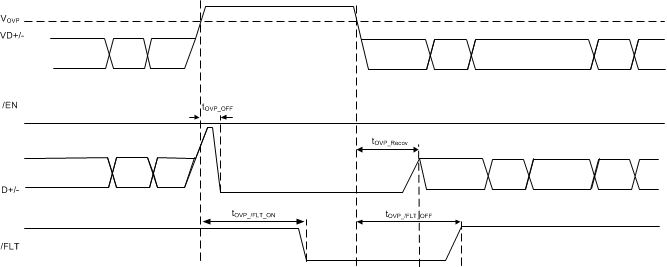
| tOVP_response_VBUS | OVP response time to VBUS | Mode 0 or 1. Measured from OVP condition to FET turn off . Short VD± to 5 V and measure the time it takes D± voltage to reach 0.1 × VD±_CLAMP_MAX from the time the 5-V hot-plug is applied. RLOAD_D± = 45 Ω.(1)(2) | 2 | µs | ||
| tOVP_response | OVP response time | Mode 0 or 1. Measured from OVP condition to FET turn off . Short VD± to 18 V and measure the time it takes D± voltage to reach 0.1 × VD±_CLAMP_MAX from the time the 18-V hot-plug is applied. RLOAD_D± = 45 Ω(1)(2) | 0.1 | 1 | µs | |
| tOVP_Recov_FLT | Recovery time FLT pin | Measured from OVP clear to FLT deassertion(1) | 32 | ms | ||
| tOVP_Recov_FET | Recovery time for data FET to turn back on | Measured from OVP clear until FET turns back on. Drop VD+ from 16 V to 3.3 V with VREF = 3.3 V, measure time it takes for D+ to reach 90% of 3.3 V | 32 | ms | ||
| tOVP_ASSERT | FLT assertion time | Measured from OVP on VD+ or VD– to FLT assertion | 12.6 | 18 | 23.4 | ms |
(1) Shown in Figure 1.
(2) Specified by design, not production tested.

1. OVP Operation – VD+, VD–
Figure 1. TPD2S703-Q1 Timing Diagram