SCAS339T March   1994  – May 2024 SN74LVC126A

PRODUCTION DATA  

  1.   1
  2. Features
  3. Applications
  4. Description
  5. Pin Configuration and Functions
  6. Specifications
    1. 5.1 Absolute Maximum Ratings
    2. 5.2 ESD Ratings
    3. 5.3 Recommended Operating Conditions
    4. 5.4 Thermal Information
    5. 5.5 Electrical Characteristics
    6. 5.6 Switching Characteristics
    7. 5.7 Typical Characteristics
  7. Parameter Measurement Information
  8. Detailed Description
    1. 7.1 Overview
    2. 7.2 Functional Block Diagram
    3. 7.3 Feature Description
    4. 7.4 Device Functional Modes
  9. Application and Implementation
    1. 8.1 Application Information
    2. 8.2 Typical Application
      1. 8.2.1 Design Requirements
      2. 8.2.2 Detailed Design Procedure
      3. 8.2.3 Application Curve
    3. 8.3 Power Supply Recommendations
    4. 8.4 Layout
      1. 8.4.1 Layout Guidelines
      2. 8.4.2 Layout Example
  10. Device and Documentation Support
    1. 9.1 Documentation Support
      1. 9.1.1 Related Documentation
    2. 9.2 Receiving Notification of Documentation Updates
    3. 9.3 Support Resources
    4. 9.4 Trademarks
    5. 9.5 Electrostatic Discharge Caution
    6. 9.6 Glossary
  11. 10Revision History
  12. 11Mechanical, Packaging, and Orderable Information

封装选项

机械数据 (封装 | 引脚)
散热焊盘机械数据 (封装 | 引脚)
订购信息

Parameter Measurement Information

Phase relationships between waveforms were chosen arbitrarily for the examples listed in the following table. All input pulses are supplied by generators having the following characteristics: PRR ≤ 1MHz, ZO = 50Ω, tt ≤ 2.5ns.

The outputs are measured individually with one input transition per measurement.

TEST S1 S2 RL CL ΔV VLOAD
tPLH, tPHL OPEN OPEN 500Ω 50pF
tPLZ, tPZL CLOSED OPEN 500Ω 50pF 0.3V 2×VCC
tPHZ, tPZH OPEN CLOSED 500Ω 50pF 0.3V

VCC Vt RL CL ΔV VLOAD
1.8V ± 0.15V VCC/2 1kΩ 30pF 0.15V 2×VCC
2.5V ± 0.2V VCC/2 500Ω 30pF 0.15V 2×VCC
2.7V 1.5V 500Ω 50pF 0.3V 6V
3.3V ± 0.3V 1.5V 500Ω 50pF 0.3V 6V

SN74LVC126A Load Circuit for 3-State
                        Outputs
(1) CL includes probe and test-fixture capacitance.
Figure 6-1 Load Circuit for 3-State Outputs
SN74LVC126A Voltage Waveforms
                        Propagation Delays
(1) The greater between tPZL and tPZH is the same as ten.
(2) The greater between tPLZ and tPHZ is the same as tdis.
Figure 6-3 Voltage Waveforms Propagation Delays
SN74LVC126A Voltage Waveforms
                        Propagation Delays
(1) The greater between tPLH and tPHL is the same as tpd.
Figure 6-2 Voltage Waveforms Propagation Delays
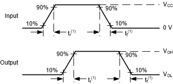
SN74LVC126A Voltage Waveforms, Input
                        and Output Transition Times
(1) The greater between tr and tf is the same as tt.
Figure 6-4 Voltage Waveforms, Input and Output Transition Times