ZHCSUW0D March 1998 – February 2024 LMC660 , LMC662
PRODUCTION DATA
- 1
- 1特性
- 2应用
- 3说明
- 4Pin Configuration and Functions
- 5Specifications
- 6Application and Implementation
- 7Device and Documentation Support
- 8Revision History
- 9Mechanical, Packaging, and Orderable Information
封装选项
机械数据 (封装 | 引脚)
散热焊盘机械数据 (封装 | 引脚)
- D|8
订购信息
6.1.2 Compensating Input Capacitance
The high input resistance of the LMC66x op amps allows the use of large feedback and source resistor values without losing gain accuracy due to loading. However, the circuit can be especially sensitive to the layout when these large-value resistors are used.
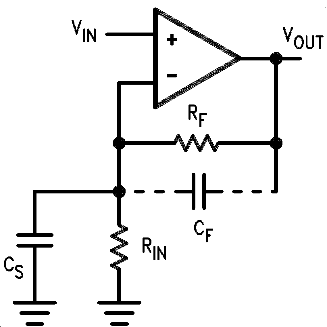
Every amplifier has some capacitance between each input and ac ground, and also some differential capacitance between the inputs. When the feedback network around an amplifier is resistive, this input capacitance (along with any additional capacitance due to circuit board traces, the socket, and so on) and the feedback resistors create a pole in the feedback path. In Figure 6-2, the frequency of this pole is:
where
- CS is the total capacitance at the inverting input, including amplifier input capacitance and any stray capacitance from the IC socket (if one is used), circuit board traces, and so on.
- RP is the parallel combination of RF and RIN.
This formula, as well as the next formula, apply to inverting and noninverting op amp configurations.
When the feedback resistors are smaller than a few kΩ, the frequency of the feedback pole can be quite high, because CS is generally less than 10pF. If the frequency of the feedback pole is much greater than the ideal closed-loop bandwidth (the nominal closed-loop bandwidth in the absence of CS), the pole can have a negligible effect on stability, as only a small amount of phase shift is added.
However, if the feedback pole is less than approximately 6 to 10 times the ideal −3dB frequency, connect a feedback capacitor, CF, between the output and the inverting input of the op amp. This condition can also be stated in terms of the amplifier low-frequency noise gain. To maintain stability, a feedback capacitor is probably be needed if:
where
is the amplifier low-frequency noise gain and GBW is the amplifier gain bandwidth product. An amplifier low-frequency noise gain is represented by the following formula, regardless of whether the amplifier is being used in an inverting or noninverting mode:
A feedback capacitor is more likely to be needed when the noise gain is low, the feedback resistor is large, or both.
If the previous condition is met (indicating that a feedback capacitor is probably needed), and the noise gain is large enough that:
the following value of feedback capacitor is recommended:
If , then set the feedback capacitor to:
These capacitor values are usually significantly smaller than those given by the older, more conservative formula:

Using the smaller capacitors provides much higher bandwidth with little degradation of transient response. In any of the previous cases, the use a somewhat larger feedback capacitor can be necessary to allow for unexpected stray capacitance, or to tolerate additional phase shifts in the loop, or excessive capacitive load, or to decrease the noise or bandwidth, or simply because the particular circuit implementation needs more feedback capacitance to be sufficiently stable. For example, a printed circuit board (PCB) stray capacitance can be larger or smaller than the breadboard stray capacitance, so the actual preferred value for CF can be different from the one estimated using the breadboard. In most cases, check the value of CF on the actual circuit, starting with the computed value.