ZHCSUW0D March 1998 – February 2024 LMC660 , LMC662
PRODUCTION DATA
- 1
- 1特性
- 2应用
- 3说明
- 4Pin Configuration and Functions
- 5Specifications
- 6Application and Implementation
- 7Device and Documentation Support
- 8Revision History
- 9Mechanical, Packaging, and Orderable Information
封装选项
机械数据 (封装 | 引脚)
散热焊盘机械数据 (封装 | 引脚)
- D|8
订购信息
6.2 Typical Applications
Additional single-supply applications ideas can be found in the LM358 data sheet. The LMC66x is pin-for-pin compatible with the LM358 and offers greater bandwidth and input resistance over the LM358. These features can improve the performance of many existing single-supply applications. Be aware, however, that the supply voltage range of the LM662 is smaller than that of the LM358.
 Figure 6-6 Low Leakage Sample and
Hold
Figure 6-6 Low Leakage Sample and
Hold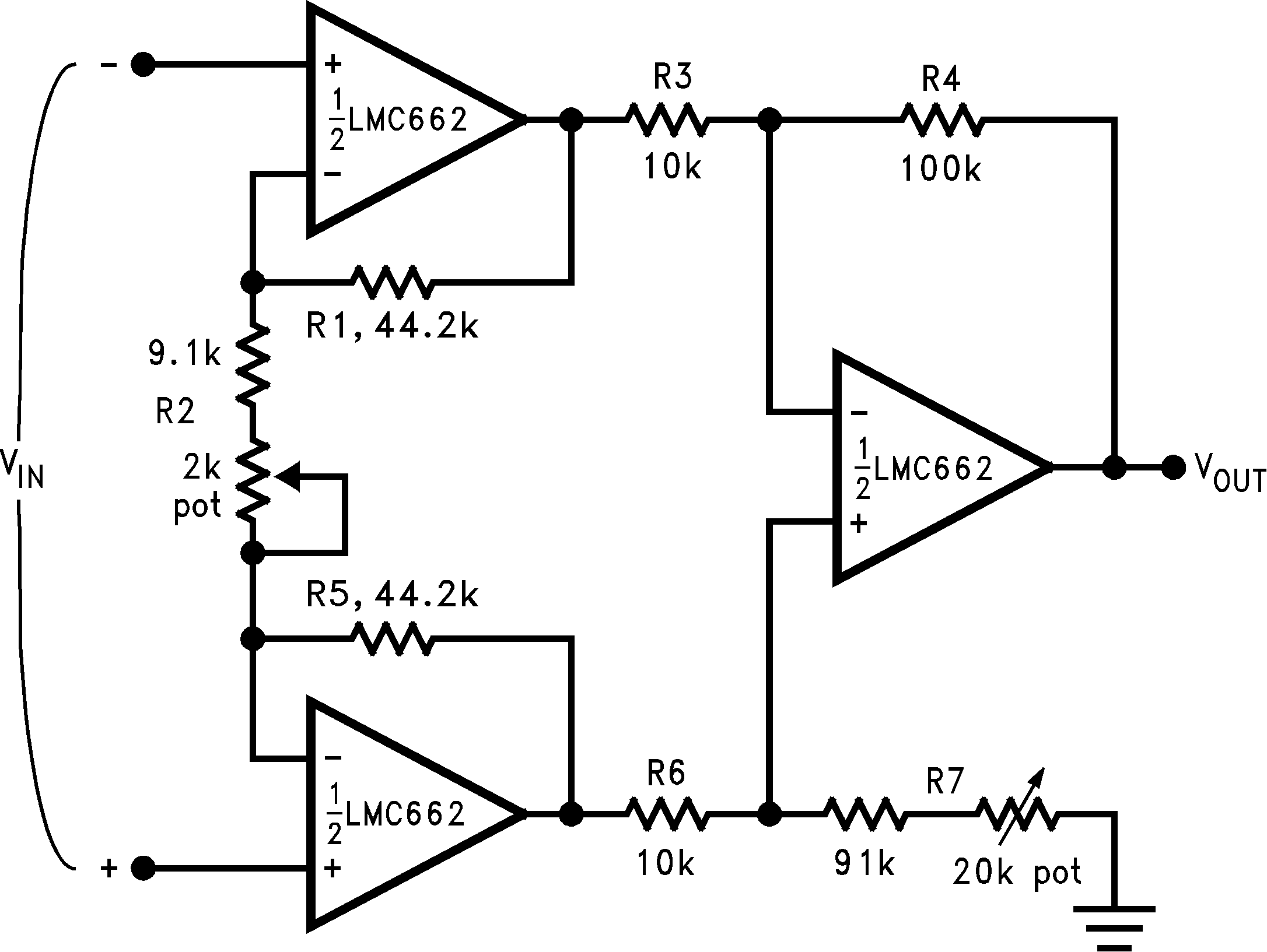
 Figure 6-7 Instrumentation Amplifier
Use low drift resistors for good CMRR performance over temperature. Matching of R3 to R6 and R4 to R7 affects CMRR. Gain can be adjusted through R2. CMRR can be adjusted through R7. An improved circuit can be designed using the RES11A-Q1, low drift, precision matched resistor pairs. A precise gain of 99 is easily implemented as shown in Figure 6-8.
 Figure 6-8 Improved
Instrumentation Amplifier With the RES11A
Figure 6-8 Improved
Instrumentation Amplifier With the RES11A
fOSC = 1/2πRC
where R = R1 = R2 and C = C1 = C2.
This circuit, as shown, oscillates at 2.0kHz with a peak-to-peak output swing of 4.5V.
 Figure 6-10 1Hz
Square-Wave Oscillator
Figure 6-10 1Hz
Square-Wave Oscillator Figure 6-11 Power
Amplifier
Figure 6-11 Power
Amplifier
| fO = 10Hz, Q = 2.1, gain = −8.8 |

| fc = 10Hz, d = 0.895, gain = 1, 2dB pass-band ripple |
") Figure 6-14 1Hz
Low Pass Filter
Figure 6-14 1Hz
Low Pass Filter(Maximally Flat, Dual Supply Only)

| Gain = −46.8 Output offset voltage reduced to the level of the input offset voltage of the bottom amplifier (typically 1mV). |
Offset Voltage Reduction