ZHCSIZ1G May 2010 – November 2018 LM98640QML-SP
PRODUCTION DATA.
- 1 特性
- 2 应用
- 3 说明
- 4 修订历史记录
- 5 Pin Configuration and Functions
- 6 Specifications
-
7 Detailed Description
- 7.1 Overview
- 7.2 Functional Block Diagram
- 7.3 Feature Description
- 7.4
Device Functional Mode
- 7.4.1 Powerdown Modes
- 7.4.2
LVDS Test Modes
- 7.4.2.1 Test Mode 0 - Fixed Pattern
- 7.4.2.2 Test Mode 1 - Horizontal Gradient
- 7.4.2.3 Test Mode 2 - Vertical Gradient
- 7.4.2.4 Test Mode 3 - Lattice Pattern
- 7.4.2.5 Test Mode 4 - Stripe Pattern
- 7.4.2.6 Test Mode 5 - LVDS Test Pattern (Synchronous)
- 7.4.2.7 Test Mode 6 - LVDS Test Pattern (Asynchronous)
- 7.4.2.8 Pseudo Random Number Mode
- 7.5 Programming
- 7.6 Register Maps
- 8 Application and Implementation
- 9 Layout
- 10器件和文档支持
- 11机械、封装和可订购信息
7.3.2.1 Sample and Hold Mode Biasing
Proper DC biasing of the CCD waveform in Sample and Hold mode is critical for realizing optimal operating conditions. In Sample/Hold Mode, the DC bias point of the input pin is typically set by actuating the input clamp switch (see Figure 17) during optical black pixels which connects the input pins to the VCLP pin DC voltage. The signal controlling this switch is CLPIN. CLPIN is an external signal connected on the CLPIN pin.
Actuating the input clamp will force the average value of the CCD waveform to be centered around the VCLP DC voltage. During Optical Black Pixels, the CCD output has roughly three components. The first component of the pixel is a “Reset Noise” peak followed by the Reset (or Pedestal) Level voltage, then finally the Black Level voltage signal. Taking the average of these signal components will result in a final “clamped” DC bias point that is close to the Black Level signal voltage.
To provide a more precise DC bias point (i.e. a voltage closer to the Black Level voltage), the CLPIN pulse can be “gated” by the internally generated CLAMP clock. This resulting CLPINGATED signal is the logical “AND” of the CLAMP and CLPIN signals as shown in Figure 18. By using the CLPINGATED signal, the higher Reset Noise peak will not be included in the clamping period and only the Pedestal Level components of the CCD waveform will be centered around VCLP.
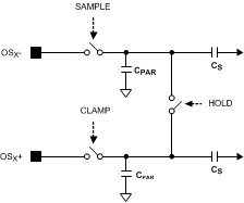
 Figure 19. Sample and Hold Mode Simplified Input Diagram
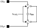
 In Sample and Hold Mode, the impedance of the analog input pins is dominated by the switched capacitance of the CDS/Sample and Hold amplifier. The amplifier switched capacitance, shown as CS in Figure 19, and internal parasitic capacitances can be estimated by a single capacitor switched between the analog input and the VCLP reference pin for Sample and Hold mode. During each pixel cycle, the modeled capacitor, CSH, is charged to the OSX+ minus OSX– voltage then discharged. The average input current at the OSX– pin can be calculated knowing the input signal amplitude and the frequency of the pixel.
 Figure 20. Equivalent Input Switched Capacitance S/H Mode