ZHCSIZ1G May 2010 – November 2018 LM98640QML-SP
PRODUCTION DATA.
- 1 特性
- 2 应用
- 3 说明
- 4 修订历史记录
- 5 Pin Configuration and Functions
- 6 Specifications
-
7 Detailed Description
- 7.1 Overview
- 7.2 Functional Block Diagram
- 7.3 Feature Description
- 7.4
Device Functional Mode
- 7.4.1 Powerdown Modes
- 7.4.2
LVDS Test Modes
- 7.4.2.1 Test Mode 0 - Fixed Pattern
- 7.4.2.2 Test Mode 1 - Horizontal Gradient
- 7.4.2.3 Test Mode 2 - Vertical Gradient
- 7.4.2.4 Test Mode 3 - Lattice Pattern
- 7.4.2.5 Test Mode 4 - Stripe Pattern
- 7.4.2.6 Test Mode 5 - LVDS Test Pattern (Synchronous)
- 7.4.2.7 Test Mode 6 - LVDS Test Pattern (Asynchronous)
- 7.4.2.8 Pseudo Random Number Mode
- 7.5 Programming
- 7.6 Register Maps
- 8 Application and Implementation
- 9 Layout
- 10器件和文档支持
- 11机械、封装和可订购信息
7.3.1.2.2 CDS Mode CLAMP/SAMPLE Adjust
In CDS mode, the LM98640QML-SP utilizes two input networks, alternating between them every pixel, to increase throughput speeds. Because of this, there are two sets of CLAMP and SAMPLE windows defined in Table 8, one for even pixels and one for odd. Sample Start and Sample End Registers (0x22,0x23) along with the Clamp Start and Clamp End Registers (0x20,0x21) control both the even and odd CLAMP and SAMPLE pulses. To adjust the CLAMP and SAMPLE pulses, first send the CLAMPODD and SAMPLEODD signals to the DTM pins by writing 10 to bits[4:3] of the Clock Monitor Register (0x09). This will allow the user to observe the CLAMPODD and SAMPLEODD pulses on pins DTM0 and DTM1 along with the image sensor output using an oscilloscope. The CLAMP and SAMPLE pulses will only be shown for every other pixel because of the even odd architecture, but the positions of the even CLAMP and SAMPLE pulses will be identically defined to that of the odd CLAMP and SAMPLE; however, odd and even path mismatch could result in a slightly different position of the pulses. Then, using the Clamp Start/End and Sample Start/End registers, adjust the positions of the CLAMP and SAMPLE pulses to align them over the Reference and Video Levels of the input signal. To allow for settling and to reduce noise, the CLAMP and SAMPLE pulses should be made as wide as possible and placed near the far edge of their respective input levels.
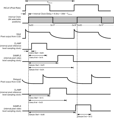
The following figure shows some examples of input CCD waveforms and placement of the CLAMP and SAMPLE positions for each. Ideally the CCD output would line up directly with the input clock at the AFE inputs, but due to trace delays in the system the CCD output is delayed relative to the input clock. In the Delayed CCD waveform the Sample Start/End Register values are lower than the Clamp Start/End Register Values. In this situation the sample pulse is not generated until the next clock period, which allows it to be correctly placed in the Video Level of the input signal. Notice that edge zero of the internal clock does not line up with the rising edge of the input clock. This is due to internal delays of the clock signals. The amount of delay can be calculated from operating frequency using the following formula: tDCLK = 6.0 ns + 3 / 64 × TINCLK
 Figure 16. CDS Mode CLAMP/SAMPLE Adjust