SNVS837B June 2013 – April 2016 LM3263
PRODUCTION DATA.
- 1 Features
- 2 Applications
- 3 Description
- 4 Revision History
- 5 Pin Configuration and Functions
- 6 Specifications
-
7 Detailed Description
- 7.1 Overview
- 7.2 Functional Block Diagram
- 7.3
Feature Description
- 7.3.1 PWM Operation
- 7.3.2 PFM Operation
- 7.3.3 Active Current Assist and Analog Bypass (ACB)
- 7.3.4 Bypass Operation
- 7.3.5 Dynamic Adjustment of Output Voltage
- 7.3.6 DC-DC Operating Mode Selection
- 7.3.7 Internal Synchronous Rectification
- 7.3.8 Current Limit
- 7.3.9 Timed Current Limit
- 7.3.10 Thermal Overload Protection
- 7.3.11 Start-Up
- 7.4 Device Functional Modes
- 7.5 Programming
- 7.6 Register Map
- 8 Application Information
- 9 Power Supply Recommendations
- 10Layout Considerations
- 11Device and Documentation Support
- 12Mechanical, Packaging, and Orderable Information
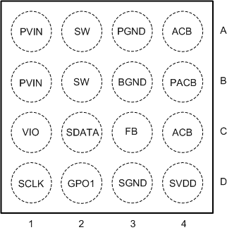
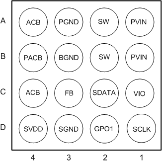
5 Pin Configuration and Functions
YFQ Package
16-Pin DSBGA
Top View

YFQ Package
16-Pin DSBGA
Bottom View

Pin Functions
| PIN | TYPE | DESCRIPTION | |
|---|---|---|---|
| NAME | NUMBER | ||
| ACB | A4 | Output | ACB and analog bypass output. Connect to the output at the output filter capacitor. |
| C4 | |||
| BGND | B3 | Ground | ACB, analog bypass ground, and digital ground. |
| FB | C3 | Input | Feedback analog input. Connect to the output at the output filter capacitor. |
| GPO1 | D2 | Output | General purpose output. Also used to reconfigure USID. |
| PACB | B4 | Power | ACB power supply input |
| PGND | A3 | Ground | Power ground to the internal NFET switch |
| PVIN | A1 | Power | Power supply voltage input to the internal PFET switch |
| B1 | |||
| SCLK | D1 | Digital/Input | Digital control interface RFFE Bus clock input. Typically connected to RFFE master on RF or baseband IC. SCLK must be held low when VIO is not applied. |
| SDATA | C2 | Digital Input/Output | Digital control interface RFFE bus data input/output. Typically connected to RFFE master on RF or baseband IC. SDATA must be held low when VIO is not applied. |
| SGND | D3 | Ground | Signal analog ground (low current) |
| SVDD | D4 | Power | Analog power supply voltage |
| SW | A2 | Analog | Switching node connection to the internal PFET switch and NFET synchronous rectifier. |
| B2 | |||
| VIO | C1 | Input | VIO functions as the RFFE interface reference voltage. VIO also functions as reset and enable input to the LM3263. Typically connected to voltage regulator controlled by RF or baseband IC. |