SNVS837B June 2013 – April 2016 LM3263
PRODUCTION DATA.
- 1 Features
- 2 Applications
- 3 Description
- 4 Revision History
- 5 Pin Configuration and Functions
- 6 Specifications
-
7 Detailed Description
- 7.1 Overview
- 7.2 Functional Block Diagram
- 7.3
Feature Description
- 7.3.1 PWM Operation
- 7.3.2 PFM Operation
- 7.3.3 Active Current Assist and Analog Bypass (ACB)
- 7.3.4 Bypass Operation
- 7.3.5 Dynamic Adjustment of Output Voltage
- 7.3.6 DC-DC Operating Mode Selection
- 7.3.7 Internal Synchronous Rectification
- 7.3.8 Current Limit
- 7.3.9 Timed Current Limit
- 7.3.10 Thermal Overload Protection
- 7.3.11 Start-Up
- 7.4 Device Functional Modes
- 7.5 Programming
- 7.6 Register Map
- 8 Application Information
- 9 Power Supply Recommendations
- 10Layout Considerations
- 11Device and Documentation Support
- 12Mechanical, Packaging, and Orderable Information
10 Layout Considerations
10.1 Layout Guidelines
10.1.1 1. Overview
PC board layout is critical to successfully designing a DC-DC converter into a product. A properly planned board layout optimizes the performance of a DC-DC converter and minimizes effects on surrounding circuitry while also addressing manufacturing issues that can have adverse impacts on board quality and final product yield.
10.1.2 2. PCB
Poor board layout can disrupt the performance of a DC-DC converter and surrounding circuitry by contributing to EMI, ground bounce, and resistive voltage loss in the traces. Erroneous signals could be sent to the DC-DC converter device, resulting in poor regulation or instability. Poor layout can also result in re-flow problems leading to poor solder joints between the DSBGA package and board pads. Poor solder joints can result in erratic or degraded performance of the converter.
10.1.2.1 Energy Efficiency
Minimize resistive losses by using wide traces between the power components and doubling up traces on multiple layers when possible.
10.1.2.2 EMI
By its very nature, any switching converter generates electrical noise. The circuit board designer’s challenge is to minimize, contain, or attenuate such switcher-generated noise. A high-frequency switching converter, such as the LM3263, switches Ampere level currents within nanoseconds, and the traces interconnecting the associated components can act as radiating antennas. The following guidelines are offered to help to ensure that EMI is maintained within tolerable levels.
To help minimize radiated noise:
- Place the LM3263 DC-DC converter, its input capacitor, and output filter inductor and capacitor close together, and make the interconnecting traces as short as possible.
- Arrange the components so that the switching current loops curl in the same direction. During the first half of each cycle, current flows from the input filter capacitor, through the internal PFET of the LM3263 and the inductor, to the output filter capacitor, then back through ground, forming a current loop. In the second half of each cycle, current is pulled up from ground, through the internal synchronous NFET of the LM3263 by the inductor, to the output filter capacitor and then back through ground, forming a second current loop. Routing these loops so the current curls in the same direction prevents magnetic field reversal between the two half-cycles and reduces radiated noise.
- Make the current loop area(s) as small as possible. Interleave doubled traces with ground planes or return paths, where possible, to further minimize trace inductances.
- The Active Current Assist and Bypass (ACB) trace must be kept short and routed directly from ACB pads to the VOUT pad at the inductor.
To help minimize conducted noise in the ground-plane:
- Reduce the amount of switching current that circulates through the ground plane — connect PGND bump of the LM3263 and its input filter capacitor together using generous component-side copper fill as a pseudo-ground plane. Then connect this copper fill to the system ground-plane (if one is used) by multiple vias located at the input filter capacitor ground terminal. The multiple vias help to minimize ground bounce at the LM3263 by giving it a low-impedance ground connection. Do not route the PGND pad directly to the RF ground plane.
- An additional high frequency capacitor in 01005 (0402 mm) case size is also recommended between PVIN and the RF ground plane. Do not connect to PGND directly.
- For optimum RF performance connect the output capacitor ground to the RF ground or system ground plane. Do not connect to PGND directly.
To help minimize coupling to the voltage feedback trace of the DC-DC converter:
- Route noise sensitive traces, such as the voltage feedback path (FB), as directly as possible from the DC-DC converter FB pad to the VOUT pad of the output capacitor, but keep them away from noisy traces between the power components.
To help minimize noise coupled back into power supplies:
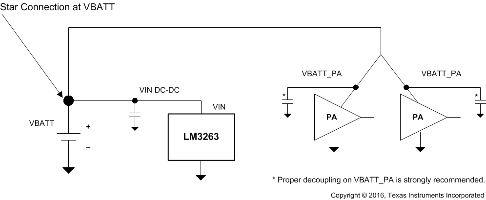
- Use a star connection to route from the VBATT power input to DC-DC converter PVIN and to VBATT_PA.
- Route traces for minimum inductance between PVIN pads and the input capacitor(s).
- Route traces to minimize inductance between the input capacitors and the ground plane.
- Maximize power supply trace inductance(s) to reduce coupling among function blocks.
- Inserting a ferrite bead in line with power supply traces can offer a favorable tradeoff in terms of board area, by attenuating noise that might otherwise propagate through the supply connections, allowing the use of fewer bypass capacitors.
10.1.3 3. Manufacturing Considerations
The LM3263 device is packaged in a 16-pin (4 × 4) array of 0.24-mm solder balls, with a 0.4-mm pad pitch. A few simple design rules go a long way to ensuring a good layout.
- Pad size must be 0.225 ± 0.02 mm. Solder mask opening must be 0.325 ± 0.02 mm.
- As a thermal relief, connect to each pad with 9-mil wide, 6-mil long traces and incrementally increase each trace to its optimal width. Symmetry is important to ensure the solder bumps re-flow evenly. Refer toAN-1112 DSBGA Wafer Level Chip Scale Package (SNVA009).
10.2 4. Layout Examples
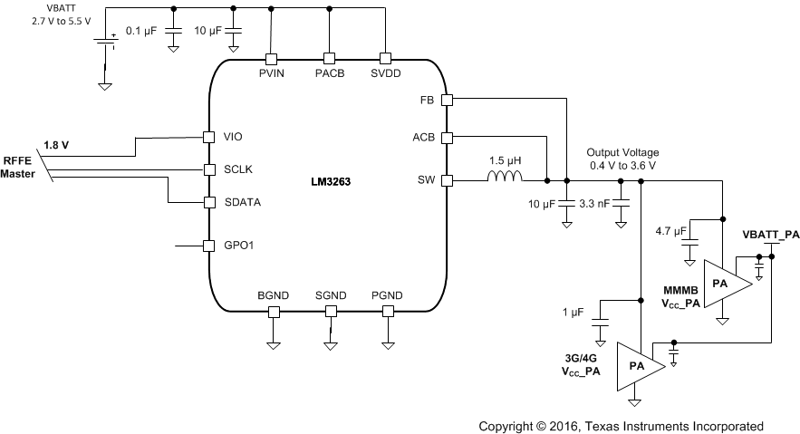 Figure 30. Simplified LM3263 RF Evaluation Board Schematic
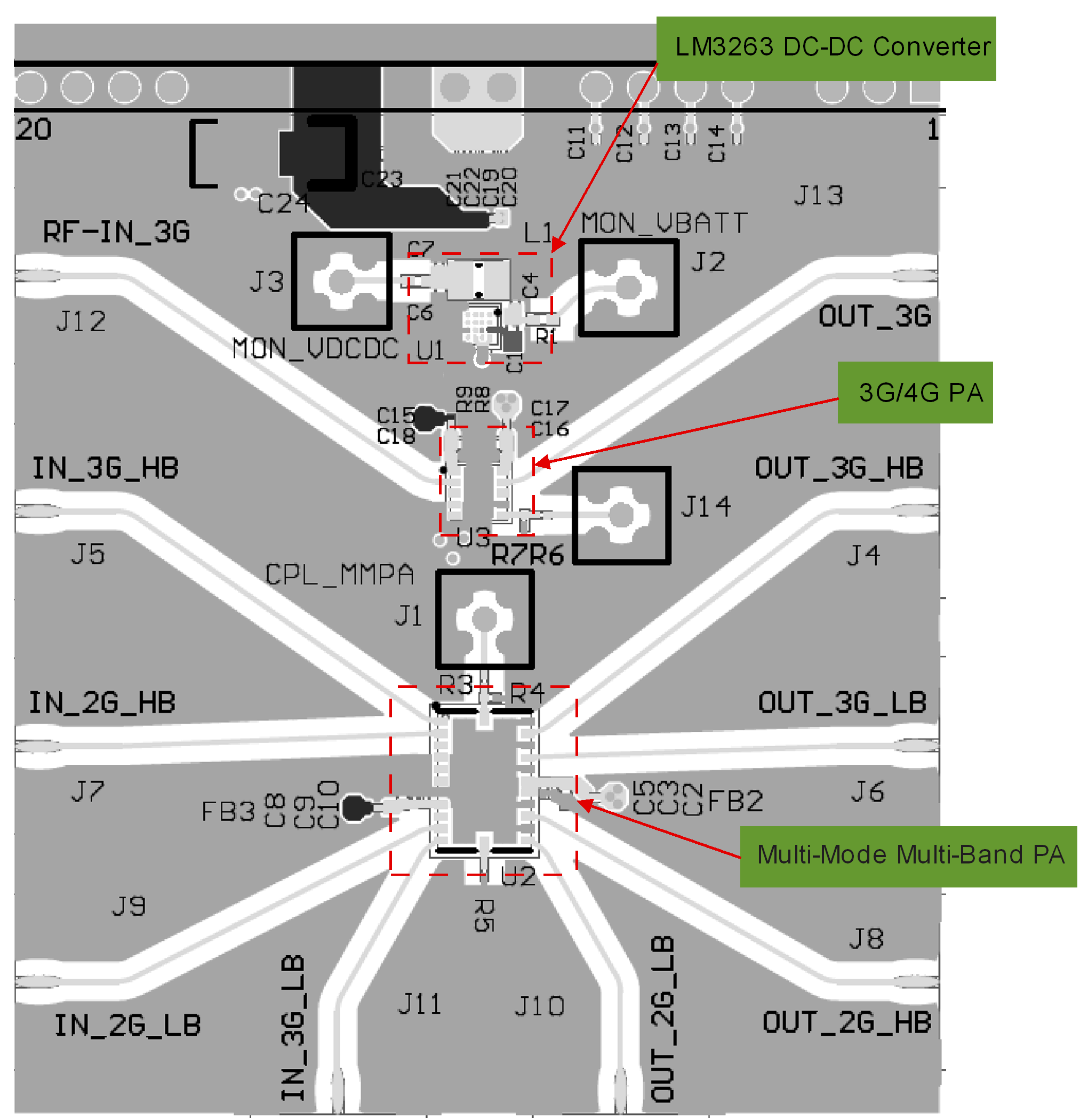 Figure 31. Top View of RF Evaluation Board With PAs
10.2.1 DC-DC Converter
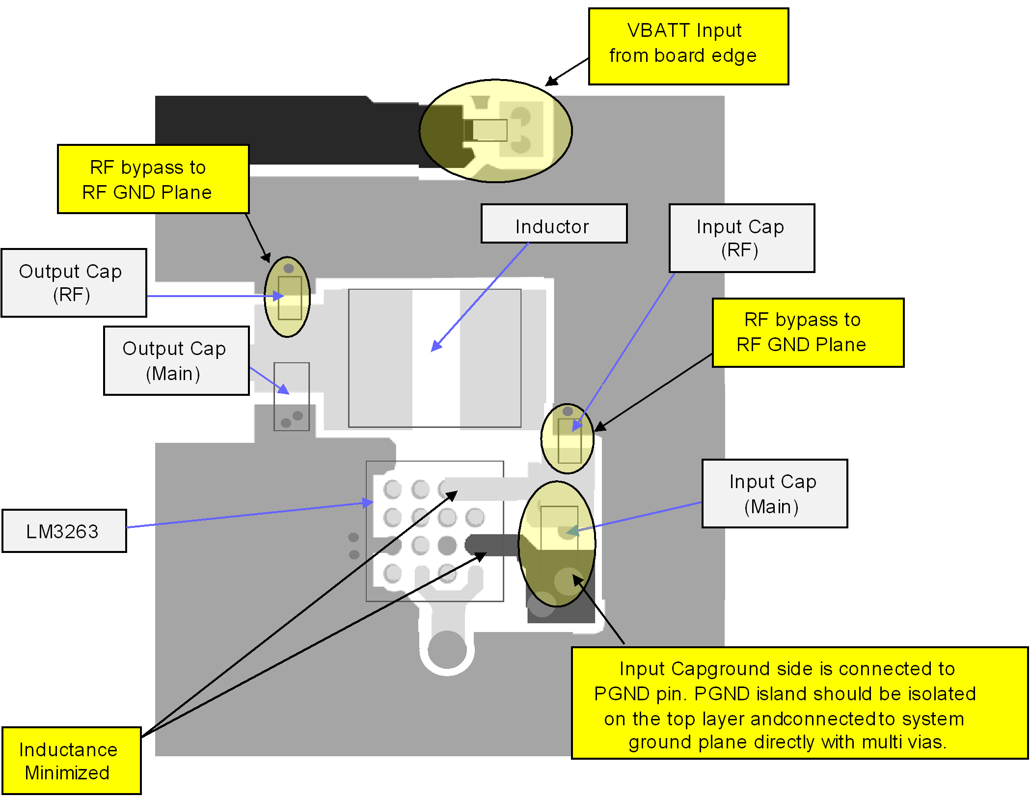 Figure 32. Top Layer
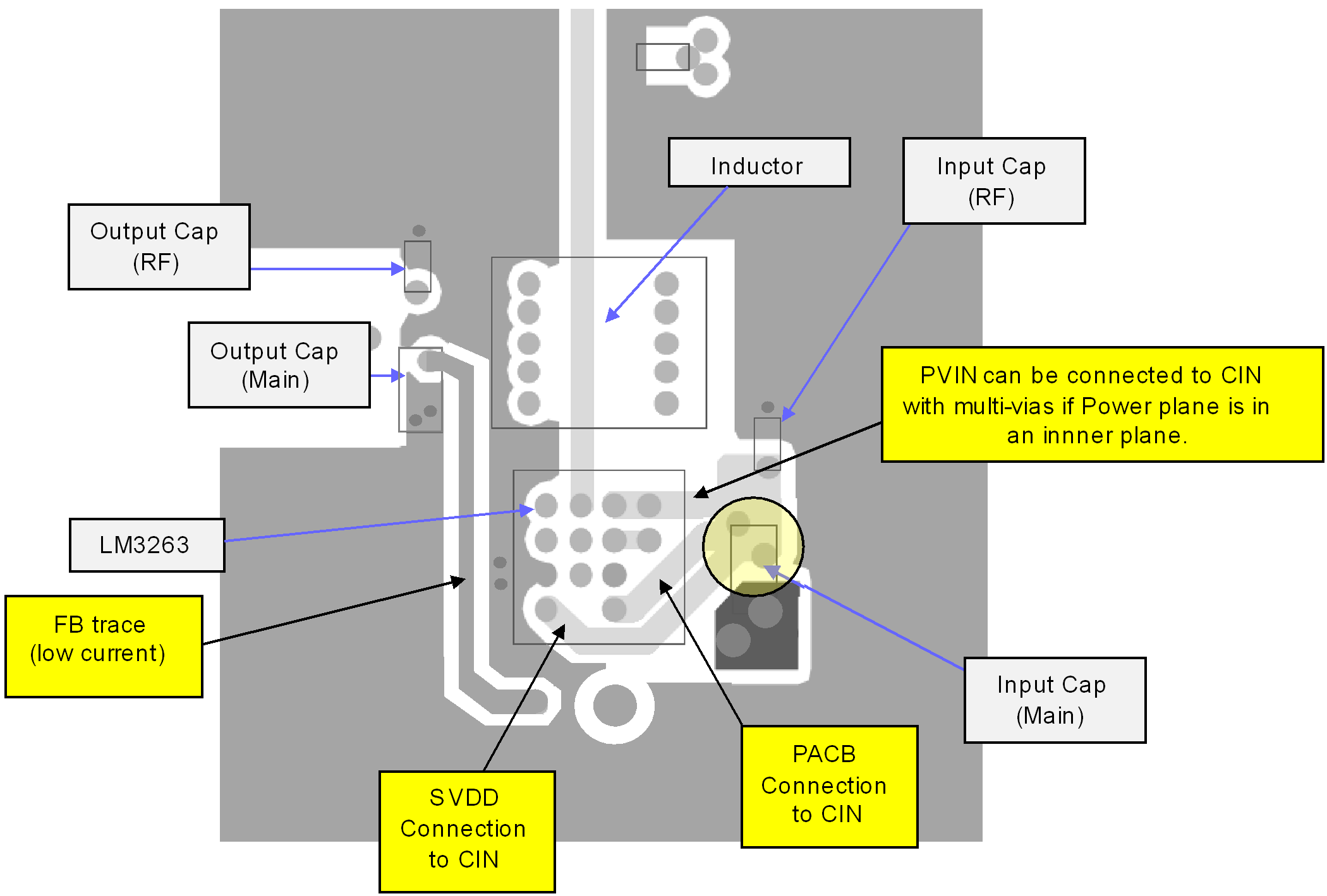 Figure 33. Board Layer 2 – FB, SVDD, PACB, PVIN
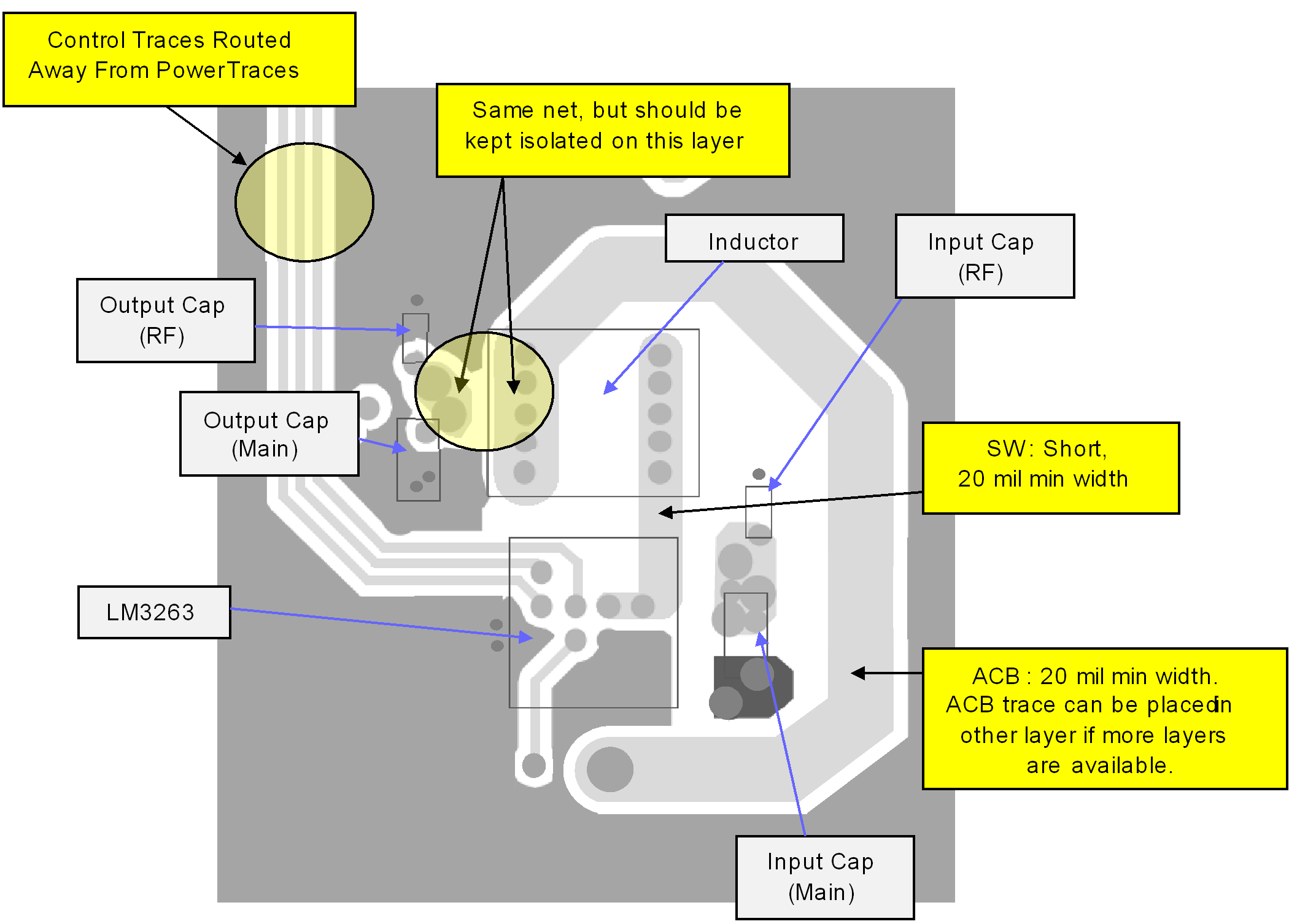 Figure 34. Board Layer 3 – SW, ACB
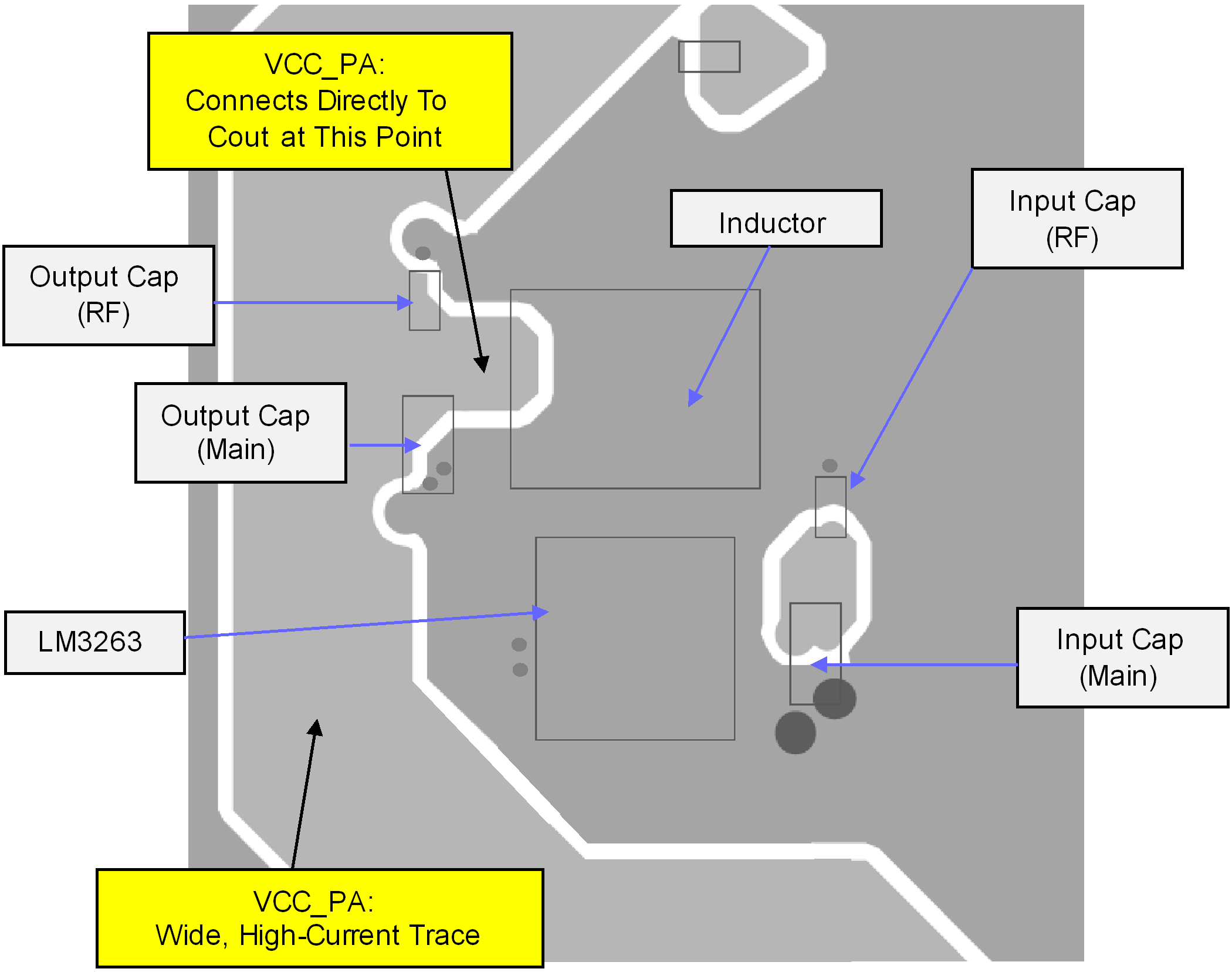 Figure 35. Board Layer 4 – VCC_PA, System GND Plane
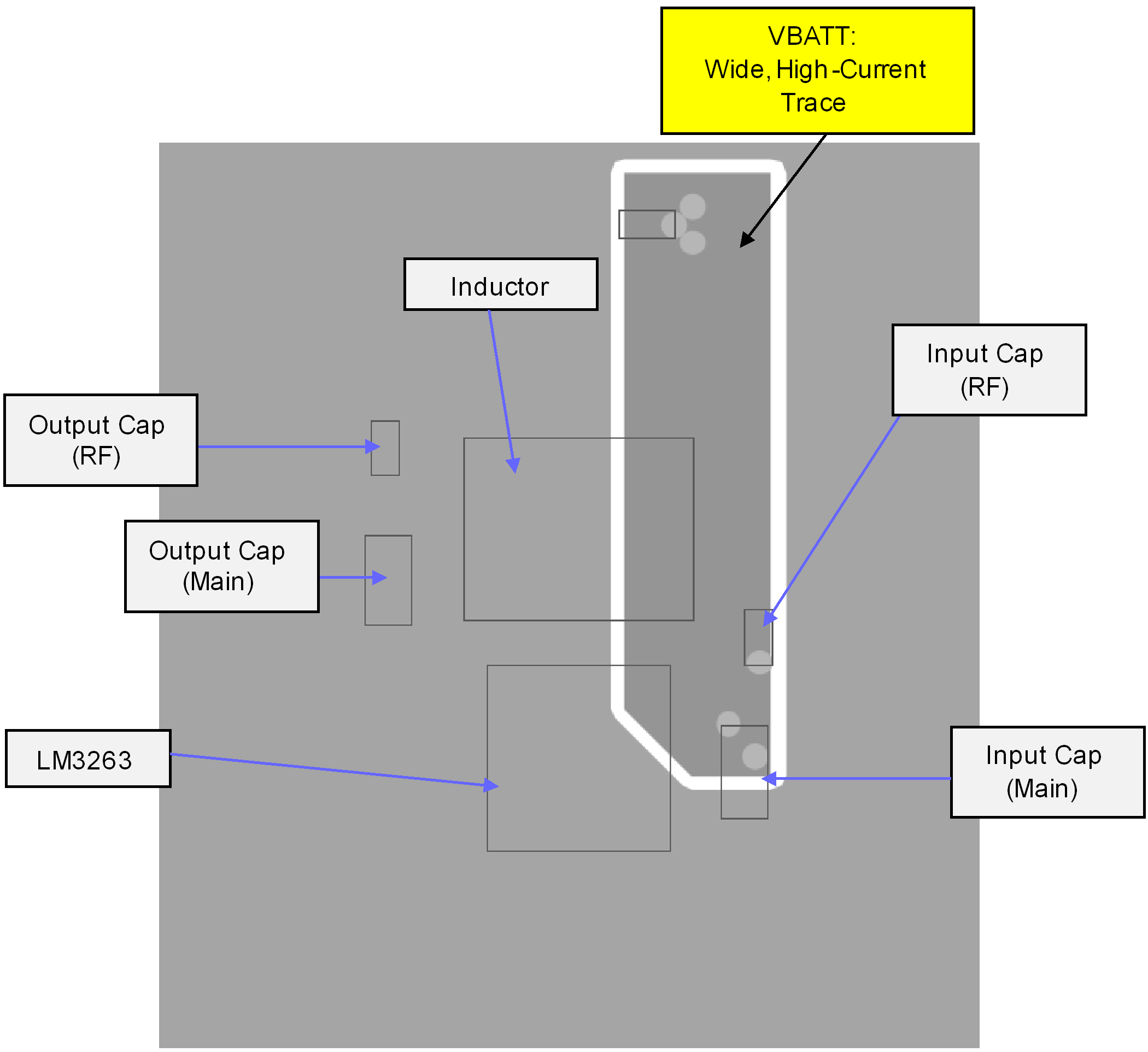 Figure 36. Board Layer 5 – VBATT Connection
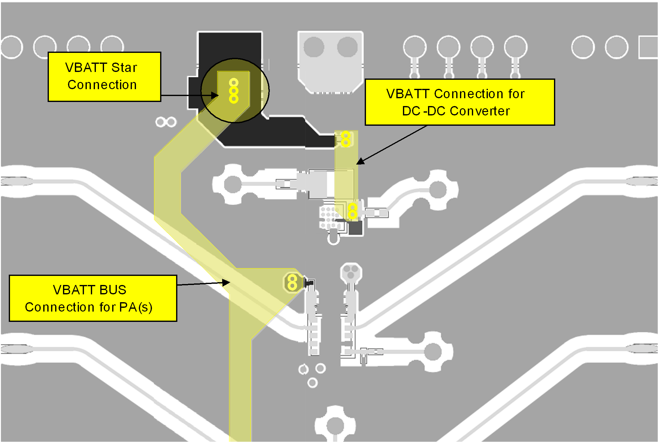 Figure 37. Multiple Board Layers – VBATT Supply Star Connection
10.2.1.1 Star Connection Between VBATT, DC-DC Converter, and PA
10.3 DSBGA Package Assembly and Use
Use of the DSBGA package requires specialized board layout, precision mounting, and careful re-flow techniques, as detailed in AN-1112 DSBGA Wafer Level Chip Scale Package (SNVA009). Refer to the section Surface Mount Technology (SMD) Assembly Considerations. For best results in assembly, alignment ordinals on the PC board must be used to facilitate placement of the device. The pad style used with DSBGA package must be the NSMD (non-solder mask defined) type. This means that the solder-mask opening is larger than the pad size. This prevents a lip that otherwise forms if the solder-mask and pad overlap from holding the device off the surface of the board and interfering with mounting. See SNVA009 for specific instructions how to do this.
The 16-pin package used for the LM3263 has 265 micron (nominal) solder balls and requires 0.225-mm pads for mounting the circuit board. The trace to each pad must enter the pad with a 90° entry angle to prevent debris from being caught in deep corners. Initially, the trace to each pad must be about 0.142-mm wide, for a section approximately 0.127-mm long, as a thermal relief. Then each trace must neck up or down to its optimal width.
An important criterion is symmetry to insure the solder bumps on the LM3263 re-flow evenly and that the device solders level to the board. In particular, special attention must be paid to the pads for bumps A1, A3, B1, and B3 because PGND, PVIN and BGND are typically connected to large copper planes; inadequate thermal relief can result in inadequate re-flow of these bumps.
The DSBGA package is optimized for the smallest possible size in applications with red-opaque or infrared-opaque cases. Because the DSBGA package lacks the plastic encapsulation characteristic of larger devices, it is vulnerable to light. Backside metallization and/or epoxy coating, along with front-side shading by the printed circuit board, reduce this sensitivity. However, the package has exposed die edges that are sensitive to light in the red and infrared range shining on the exposed die edges of the package.
