SNOSC66D MARCH 2012 – September 2016 LM3017
PRODUCTION DATA.
- 1 Features
- 2 Applications
- 3 Description
- 4 Revision History
- 5 Pin Configuration and Functions
- 6 Specifications
- 7 Detailed Description
-
8 Application and Implementation
- 8.1 Application Information
- 8.2
Typical Application
- 8.2.1 Design Requirements
- 8.2.2
Detailed Design Procedure
- 8.2.2.1 Programming the Output Voltage
- 8.2.2.2 Power Inductor Selection
- 8.2.2.3 Setting the Output Current
- 8.2.2.4 Additional Slope Compensation
- 8.2.2.5 Current Limit With Additional Slope Compensation
- 8.2.2.6 Power Diode Selection
- 8.2.2.7 Low-Side MOSFET Selection (Switching MOSFET)
- 8.2.2.8 Pass MOSFET Selection (High-Side MOSFET)
- 8.2.2.9 Input Capacitor Selection
- 8.2.2.10 Output Capacitor Selection
- 8.2.2.11 VCC Decoupling Capacitor
- 8.2.2.12 Slope Compensation Ramp
- 8.2.2.13 Control Loop Compensation
- 8.2.3 Application Curve
- 9 Power Supply Recommendations
- 10Layout
- 11Device and Documentation Support
- 12Mechanical, Packaging, and Orderable Information
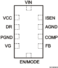
5 Pin Configuration and Functions
NKL Package
10-Pin WQFN
Top View

Pin Functions
| PIN | TYPE(1) | DESCRIPTION | ||
|---|---|---|---|---|
| NO. | NAME | |||
| 1 | VCC | O | Driver supply voltage pin: output of internal regulator powering low side NMOS driver. A minimum of 0.47 µF must be connected from this pin to PGND for proper operation. | |
| 2 | DR | O | Low-side NMOS gate driver output: output gate drive to low side NMOS gate. | |
| 3 | PGND | G | Power ground: ground for power section. External power circuit reference. Must be connected to AGND at a single point. | |
| 4 | VG | O | High side NMOS gate driver output: output gate drive to high side NMOS gate. | |
| 5 | EN/MODE | A | Multi-function input pin: this input provides for chip enable, and mode selection. See Device Functional Modes for details. | |
| 6 | FB | A | Feed-back input pin: negative input to error amplifier. Connect to feedback resistor tap to regulate output. | |
| 7 | COMP | A | Compensation pin: a resistor and capacitor combination connected to this pin provides frequency compensation for the regulator control loop. | |
| 8 | AGND | G | Analog ground: ground for analog control circuitry. Reference point for all stated voltages. | |
| 9 | ISEN | A | Current sense input: current sense input, with respect to VIN, for all current limit functions. | |
| 10 | VIN | P | Power supply input pin: input supply to regulator. See Application and Implementation for recommendations on bypass capacitors on this pin. | |
(1) A = Analog, G = Ground, O = Output, P = Power