SNOSC66D MARCH 2012 – September 2016 LM3017
PRODUCTION DATA.
- 1 Features
- 2 Applications
- 3 Description
- 4 Revision History
- 5 Pin Configuration and Functions
- 6 Specifications
- 7 Detailed Description
-
8 Application and Implementation
- 8.1 Application Information
- 8.2
Typical Application
- 8.2.1 Design Requirements
- 8.2.2
Detailed Design Procedure
- 8.2.2.1 Programming the Output Voltage
- 8.2.2.2 Power Inductor Selection
- 8.2.2.3 Setting the Output Current
- 8.2.2.4 Additional Slope Compensation
- 8.2.2.5 Current Limit With Additional Slope Compensation
- 8.2.2.6 Power Diode Selection
- 8.2.2.7 Low-Side MOSFET Selection (Switching MOSFET)
- 8.2.2.8 Pass MOSFET Selection (High-Side MOSFET)
- 8.2.2.9 Input Capacitor Selection
- 8.2.2.10 Output Capacitor Selection
- 8.2.2.11 VCC Decoupling Capacitor
- 8.2.2.12 Slope Compensation Ramp
- 8.2.2.13 Control Loop Compensation
- 8.2.3 Application Curve
- 9 Power Supply Recommendations
- 10Layout
- 11Device and Documentation Support
- 12Mechanical, Packaging, and Orderable Information
8 Application and Implementation
NOTE
Information in the following applications sections is not part of the TI component specification, and TI does not warrant its accuracy or completeness. TI’s customers are responsible for determining suitability of components for their purposes. Customers should validate and test their design implementation to confirm system functionality.
8.1 Application Information
The LM3017 may be operated in either continuous or discontinuous conduction mode. The following descriptions assume continuous conduction operation (CCM). This mode of operation has higher efficiency and lower EMI characteristics than the discontinuous mode.
8.2 Typical Application
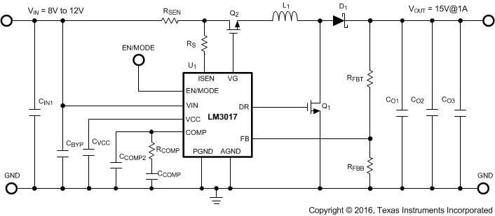 Figure 16. 1-A High Efficiency Step-Up (Boost) Converter
8.2.1 Design Requirements
To properly size the components for the application, the designer requires the following parameters: Input voltage range, output voltage, output current, and switching frequency. These four main parameters affect the choices of component available to achieve a proper system behavior.
Table 2 lists the design parameters for this application example.
Table 2. Design Parameters
| PARAMETER | VALUE |
| Input voltage, VIN | 8 V to 12 V |
| Output voltage, VOUT | 15 V |
| Output current, IOUT | 1 A |
| Switching frequency, fS | 600 kHz |
8.2.2 Detailed Design Procedure
The most common topology for the LM3017 is the boost or step-up topology. The boost converter converts a low input voltage into a higher output voltage. The basic configuration for a boost regulator is shown in Figure 17. In continuous conduction mode (when the inductor current never reaches zero at steady state), the boost regulator operates in two cycles. In the first cycle of operation, MOSFET Q is turned on and energy is stored in the inductor. During this cycle, diode D1 is reverse biased and load current is supplied by the output capacitor, COUT.
In the second cycle, MOSFET Q is off and the diode is forward biased. The energy stored in the inductor is transferred to the load and output capacitor. The ratio of these two cycles determines the output voltage. The output voltage is defined with Equation 1.

Including the voltage drop of the diode in Equation 2.

where
- D is the duty cycle of the switch
- VD1 is the forward voltage drop of the diode
The following sections describe selection of components for a boost converter.
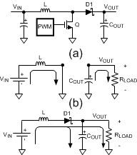 Figure 17. 4 Simplified Boost Converter Diagram
(a) First Cycle of Operation, (b) Second Cycle of Operation
8.2.2.1 Programming the Output Voltage
The output voltage can be programmed using a resistor divider between the output and the feedback pins, as shown in Figure 20. The resistors are selected such that the voltage at the feedback pin is equal to VFB (see Electrical Characteristics). RFBT and RFBB can be selected using Equation 3.

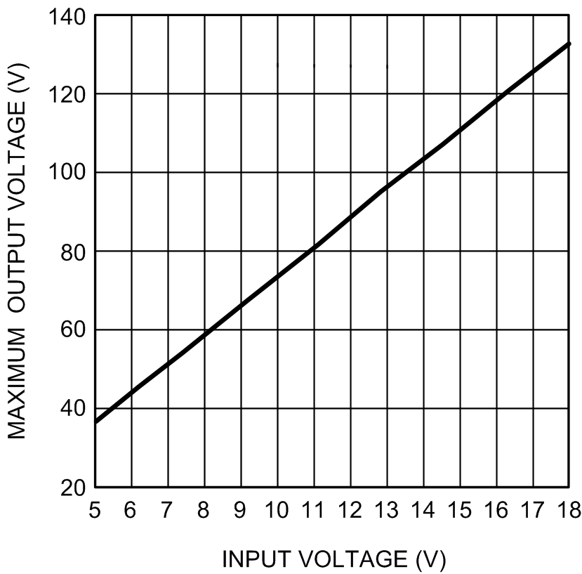 Figure 18. Maximum Output Voltage
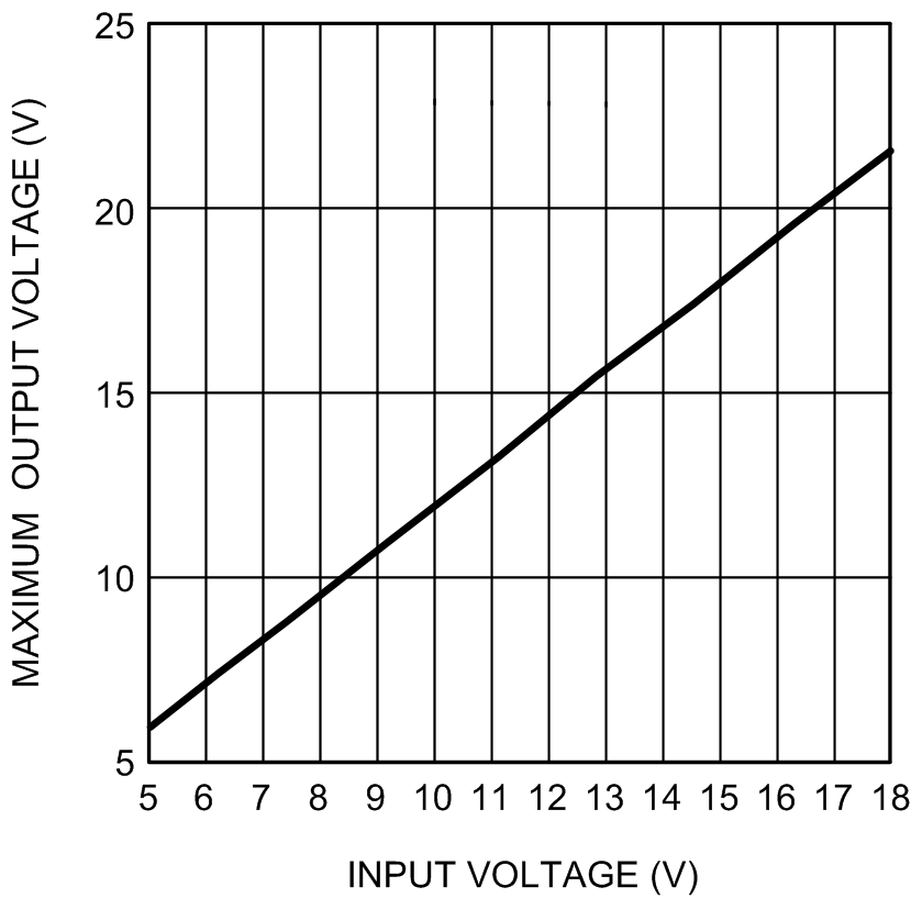 Figure 19. Minimum Output Voltage
Figure 18 shows maximum regulated output voltage based on maximum duty cycle value of 85% and by assuming a voltage drop on the output diode of 0.5 V and 90% efficiency. Figure 19 shows the minimum regulated output voltage, the calculation is based on minimum on time of 126 ns (typical) that generates a minimum duty cycle equal to Equation 4.
where
- fS is the switching frequency and it's equal to 600 kHz and by assuming 90% efficiency
8.2.2.2 Power Inductor Selection
The inductor is one of the two energy storage elements in a boost converter.
Choose the minimum IOUT to determine the minimum inductance L. A common choice is to set (2 x ΔiL) from 30% to 50% of IL. Choosing an appropriate core size for the inductor involves calculating the average and peak currents expected through the inductor. In a boost converter the inductor current IL, the peak of the inductor current and the inductor current ripple ΔiL are equal to Equation 5.
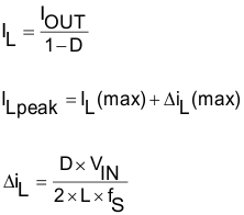
The inductance used is a tradeoff between size and cost. Larger inductance means lower input ripple current; however, because the inductor is connected to the output during the off-time only, there is a limit to the reduction in output voltage ripple. Lower inductance results in smaller, less expensive magnetics.
All the analysis in this data sheet assumes operation in continuous conduction mode. To operate in continuous conduction mode, the conditions in Equation 6 must be met.
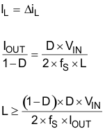
A core size with ratings higher than these values must be chosen. If the core is not properly rated, saturation dramatically reduces overall efficiency or damage the power stage. Choose an inductor with a saturation current value higher than ILpeak. The LM3017 senses the peak current through the switch. The peak current through the switch is the same as the peak current calculated in the previous equation.
Losses due to DCR of the inductance can be easily calculated with Equation 7.

No core losses are considered.
8.2.2.3 Setting the Output Current
The maximum amount of current that can be delivered at the output can be controlled by the sense resistor, RSEN. Current limit occurs when the voltage that is generated across the sense resistor equals the current sense threshold voltage, VSENSE. Limits for VSENSE are specified in Electrical Characteristics. This is expressed with Equation 8.
The peak current through the switch is equal to the peak inductor current in Equation 9.
Therefore for a boost converter in Equation 10.

Combining the two equations yields an expression for RSEN and includes a 20% margin on the peak of the switching current with Equation 11.

Evaluate RSEN at the maximum and minimum VIN values and choose the smallest RSEN calculated.
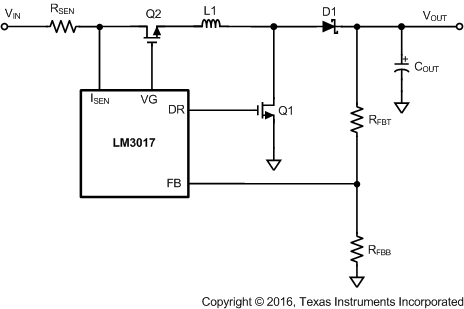 Figure 20. Adjusting the Output Voltage
8.2.2.4 Additional Slope Compensation
It is good design practice to only add as much slope compensation as required to avoid instability. Additional slope compensation (see Figure 24) minimizes the influence of the sensed current in the control loop. With very large slope compensation the control loop characteristics are similar to a voltage mode regulator which compares the error voltage to a saw tooth waveform rather than the inductor current. It is possible to calculate the minimum value of RS to meet Equation 12.
Hence Equation 13,

where
- K = 40 µA
If the result of the previous equation is negative, it means that no additional slope compensation is required. TI recommends a 100-Ω resistor.
8.2.2.5 Current Limit With Additional Slope Compensation
If an external slope compensation resistor is used, then the internal control signal is modified and this has an effect on the current limit.
If RS is used, then this adds to the existing slope compensation. The command voltage, VCS, is then given by Equation 14.
where
- VSENSE is a defined parameter in Electrical Characteristics
- VSL is the amplitude of the internal compensation ramp
- ΔVSL = RS x K is the additional slope compensation generated
This changes the equation for RSEN to Equation 15.

Because ΔVSL = RS × K as defined earlier, RS can be used to provide an additional method for setting the current limit. In some designs RS can also be used to help filter noise to keep the ISEN pin quiet. Dissipation due to RSEN resistor is equal to Equation 16.

8.2.2.6 Power Diode Selection
Observation of the boost converter circuit shows that the average current through the diode is the average output current, and the peak current through the diode is the peak current through the inductor. The peak diode current can be calculated using Equation 17.
The peak reverse voltage for a boost converter is equal to the regulator output voltage. The diode must be capable of handling this peak reverse voltage as well as the output rms current. To improve efficiency, TI recommends a low forward drop Schottky diode due to low forward drop and near-zero reverse recovery time. The overall efficiency becomes more dependent on the selection of D at low duty cycles, where the boost diode carries the load current for an increasing percentage of the time. This power dissipation can be calculated by checking the typical diode forward voltage VD, from the I-V curve on the diode's datasheet and the multiplying it by IO. Diode data sheets also provides a typical junction-to-ambient thermal resistance, RθJA, which can be used to estimate the operating die temperature of the Schottky. Multiplying the power dissipation (PD = IO × VD) by RθJA gives the temperature rise. The diode case size can then be selected to maintain the Schottky diode temperature below the operational maximum.
8.2.2.7 Low-Side MOSFET Selection (Switching MOSFET)
The drive pin, DR, of the LM3017 must be connected to the gate of an external MOSFET. In a boost topology, the drain of the external N-Channel MOSFET is connected to the inductor and the source is connected to the ground. The drive pin voltage, VDR, depends on the input voltage (see Typical Characteristics).
The selected MOSFET directly affects the efficiency. The critical parameters for selection of a MOSFET are:
- Minimum threshold voltage, VTH(MIN)
- On-resistance, RDS(ON)
- Total gate charge, Qg
- Reverse transfer capacitance, CRSS
- Maximum drain to source voltage, VDS(MAX)
The off-state voltage of the MOSFET is approximately equal to the output voltage. VDS(MAX) of the MOSFET must be greater than the output voltage plus the voltage drop across the output diode (20% margin recommended).
The power losses in the MOSFET can be categorized into conduction losses, gate charging losses and switching losses. RDS(ON) is required to estimate the conduction losses. The conduction loss, PCOND, is the I2R loss across the MOSFET. The maximum conduction loss is given by Equation 18 and Equation 19.

where
- DMAX is the maximum duty cycle

To consider the increase in MOSFET on resistance due to heating, a factor of 1.3 is introduced, hence Equation 20.
Gate charging loss, PG, results from the current required to charge and discharge the gate capacitance of the power MOSFET and is approximated with Equation 21.
QG is the total gate charge of the MOSFET. Gate charge loss differs from conduction and switching losses because the actual dissipation occurs in the LM3017 and not in the MOSFET itself. This loss, PVCC, is estimated with Equation 22.
The switching losses are very difficult to calculate due to changing parasitics of a given MOSFET in operation. Often, the individual MOSFET datasheet does not give enough information to yield a useful result. The following formulas give a rough idea how the switching losses are calculated with Equation 23.

where
- tLH and tHL are rise and fall times of the MOSFET
8.2.2.8 Pass MOSFET Selection (High-Side MOSFET)
The VG pin drives the gate of the high side MOSFET (Pass FET Q2). This requires special considerations. When the output is shorted, this FET must sustain the full input voltage and the short-circuit current simultaneously. This is due to the fact that the controller regulates the short-circuit current in a quasi-linear manner, through Q2. This power pulse only lasts for TLIM2 or TSC, depending on the operational mode. Therefore, the designer must carefully examine the SOA curve for the desired FET before committing to the design. Equation 24 and Equation 25 give the maximum energy pulses that Q2 is required to survive.


These two energy points must fall within the SOA of the selected FET. In addition, Q2 must have a low threshold voltage and low RDS(on) for high efficiency. Power dissipation during boost mode is given by Equation 26.

8.2.2.9 Input Capacitor Selection
Due to the presence of an inductor at the input of a boost converter, the input current waveform is continuous and triangular. The inductor ensures that the input capacitor sees fairly low ripple currents. However, as the input capacitor gets smaller, the input ripple goes up. The rms current in the input capacitor is given by Equation 27.

The input capacitor must be capable of handling this rms current. Although the input capacitor is not as critical in a boost application, low values can cause impedance interactions. Therefore, a good quality capacitor must be chosen in the range of 10 µF to 20 µF. Furthermore, TI recommends a low-ESR, 0.1-µF ceramic bypass capacitor to avoid transients and ringing due to parasitics. Bypass capacitors must be placed as close as possible to the VIN pin and grounded close to the GND pin on the IC to minimize additional ESR and ESL. Equation 28 can be used to define the input voltage ripple.

where
- ΔiLpp = 2 × ΔiL is the peak-to-peak inductor current ripple
- ΔVipp is the peak-to-peak input voltage ripple
Many times it is necessary to use an electrolytic capacitor on the input in parallel with the ceramics. The ESR of this capacitor can help to damp any ringing on the input supply caused by long power leads.
8.2.2.10 Output Capacitor Selection
The output capacitor in a boost converter provides all the output current when the inductor is charging and it determines the steady state output voltage ripple ΔVOpp. As a result it sees very large ripple currents. The output capacitor must be selected based on its capacitance CO, its equivalent series resistance ESR and its RMS current rating. The rms current in the output capacitor is calculated with Equation 29.

where
- ΔiL is the inductor ripple current
- D is the duty cycle
The magnitude of the output voltage ripple during the on-time is equal to the ripple voltage during the off-time and it is composed of two parts. For simplicity, the analysis is performed for off-time only.
The first part of the ripple voltage is the surge created as the output diode D turns on. At this point inductor or diode current is at the peak value, and the ripple voltage increase can be calculated with Equation 30.
where
- IPK = IOUT / (1 − D)
The second portion of the ripple voltage is the increase due to the charging of CO through the output diode. This portion can be approximated with Equation 31.
Equation 32 can be used to define the output voltage ripple.

The ESR of the output capacitor(s) has a strong influence on the slope and direction of the output voltage ripple. Capacitors with high ESR such as tantalum and aluminum electrolytic create an output voltage ripple that is dominated by ΔVO1 with a shape shown in Figure 21. Ceramic capacitors, in contrast, have a very low ESR and lower capacitance, and the shape of the output voltage ripple is dominated by ΔVO2 with a shape shown in Figure 22.
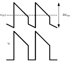 Figure 21. ΔVOpp Using High ESR Capacitors
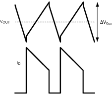 Figure 22. ΔVOpp Using Low ESR Capacitors
Ceramic capacitors are recommended with a typical value from 10 µF to 100 µF. The minimum quality dielectric that is suitable for switching power supply output capacitors is X5R, while X7R (or better) is preferred. Careful attention must be paid to the DC voltage rating and case size, as ceramic capacitors can lose 60% or more of their rated capacitance at the maximum DC voltage. This is the reason that ceramic capacitors often derate to 50% of their capacitance at their working voltage.
8.2.2.11 VCC Decoupling Capacitor
The internal bias of the LM3017 comes from either the internal bias voltage generator as shown in the block diagram or directly from the voltage at the VIN pin. At input voltages lower than 6 V, the internal IC bias is the input voltage and at voltages above 6 V the internal bias voltage generator of the LM3017 provides the bias. A good quality ceramic bypass capacitor must be connected from the VCC pin to the PGND pin for proper operation. This capacitor supplies the transient current required by the internal MOSFET driver, as well as filtering the internal supply voltage for the controller. TI recommends a value of between 0.47 µF and 4.7 µF.
8.2.2.12 Slope Compensation Ramp
The LM3017 uses a current mode control scheme. The main advantages of current mode control are inherent cycle-by-cycle current limit for the switch, simpler control loop characteristics and excellent line and load transient response. However, there is a natural instability due to subharmornic oscillations that occurs for duty cycles, D, greater than 50% if slope compensation is not addressed in Equation 33.
For best input noise immunity, use Equation 34.
For best sub-harmonic suppression, use Equation 35.
where
- MC is the slope of the compensation ramp
- M1 is the slope of the inductor current during the ON time
- M2 is the slope of the inductor current during the OFF time
- RSEN is the sensing resistor value
- VOUT represents the output voltage
- VIN represents the input voltage
- A is equal to 0.86 and it is the internal sensing amplification of the LM3017
In the case of the boost topology, use Equation 36 and Equation 37.
The compensation ramp is added internally in the LM3017. The slope of this compensation ramp is selected to satisfy most applications, and its value depends on the switching frequency. This slope can be calculated using Equation 38.
In the above equation, VSL is the amplitude of the internal compensation ramp and fS is the controller's switching frequency. Limits for VSL are specified in Electrical Characteristics.
To provide the user additional flexibility, a patented scheme is implemented inside the IC to increase the slope of the compensation ramp externally, if the requirement arises. Adding a single external resistor, RS (as shown in Figure 24) increases the amplitude of the compensation ramp as shown in Figure 23 where Equation 39.
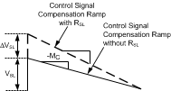 Figure 23. Additional Slope Compensation Added Using External Resistor RS
where
- K = 40 µA typically and changes slightly as the switching frequency changes
A more general equation for the slope compensation ramp, MC, is shown in Equation 40 to include ΔVSL caused by the resistor, Rs.
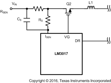 Figure 24. Increasing the Slope of the Compensation Ramp
An additional capacitor, CS, could be added if the sensing signal generated by RSEN is very noisy (parasitic circuit capacitance, inductance, and gate drive current create a spike in the current sense voltage at the point where Q1 turns on). The time constant RSEN x CS must be long enough to reduce the parasitics spike without significantly affecting the shape of the actual current sense voltage (a typical range is from 100 pF to 2.2 nF).
8.2.2.13 Control Loop Compensation
The LM3017 uses peak current-mode PWM control to correct changes in output voltage due to line and load transients. Peak current-mode provides inherent cycle-by-cycle current limiting, improved line transient response, and easier control loop compensation. The control loop is comprised of two parts. The first is the power stage, which consists of the pulse width modulator, output filter, and the load. The second part is the error amplifier. Figure 25 shows the regulator control loop components.
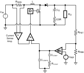 Figure 25. Power Stage and Error Amp
The power stage in a CCM peak current mode boost converter consists of the DC gain, GVC0, a single low frequency pole, fP, the ESR zero, fZ, a right-half plane zero, fR, and a double pole resulting from the sampling of the peak current. The power stage transfer function (also called the Control-to-Output transfer function) can be written with Equation 41.
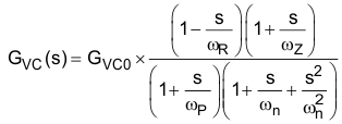
The DC gain is defined with Equation 42.

where
- RO = VOUT / IOUT
In the equation for GVC0, DC gain is highest when input voltage and output current are at the maximum. The system ESR zero is defined with Equation 43.

The low frequency pole is Equation 44.

The right-half plane zero is Equation 45.

The sampling double pole quality factor is Equation 46.

The sampling double corner frequency is Equation 47.
The natural inductor current slope is Equation 48.
The external ramp slope is Equation 49.
A step-up converter produces an undesirable right-half plane zero in the regulation feedback loop. This requires compensating the regulator such that the crossover frequency occurs well below the frequency of the right-half plane zero
8.2.2.13.1 Compensation Network Components Calculations
As shown in Figure 25, the LM3017 uses a compensation network base on a transconductance amplifier. The closed-loop transfer function is defined with Equation 50 through Equation 54.
where
- GVA(s) is the transfer function implemented by the compensation network
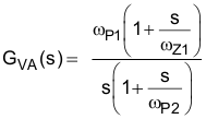


To stabilize the regulator, ensure that the regulator crossover frequency is less than or equal to one-fifth of the right-half plane zero with Equation 55.

To determine the crossover frequency it is important to note that, at that frequency, the compensation impedance (ZCOMP) is dominated by a resistor, and the output impedance (ZOUT) is dominated by the impedance of an output capacitor. Therefore, when solving for the crossover frequency, the equation (by definition of the crossover frequency) of the loop gain is simplified to Equation 56.

where
- |T| is the loop gain magnitude
- VFB is feedback voltage, 1.275 V
- VOUT is the output voltage
- VIN is the input voltage
- Gm is the error amplifier transconductance
- ZCOMP is the impedance of the compensation network from the COMP pin to ground
- RSEN is the current sensing resistor
- A is equal to 0.86 and it is the internal sensing amplification of the LM3017
- CO is the output capacitor value
Solve for RCOMP with Equation 57.

Once the compensation resistor is known, set the zero formed by the compensation capacitor and resistor to one-fourth of the crossover frequency in Equation 58.

where
- CCOMP is the compensation capacitor
The high-frequency capacitor CCOMP2, is chosen to cancel the zero introduced by output capacitance ESR with Equation 59.

For optimal transient performance, RCOMP and CCOMP might require adjustment by observing the load transient response.
For detailed explanation on how to select the right compensation components for a boost topology, see AN-1286 Compensation for the LM3478 Boost Controller (SNVA067), and AN-1994 Modeling and Design of Current Mode Control Boost Converters (SNVA408).
8.2.2.13.2 Compensation Design Example
Table 3 lists the design parameters for this application example to calculate the compensation network.
Table 3. Design Parameters
| PARAMETER | VALUE |
| Input voltage, VIN | 8 V to 12 V |
| Output voltage, VOUT | 15 V |
| Output current, IOUT | 1 A |
| Switching frequency, fS | 600 kHz |
| Duty cycle, D (considering losses) |
0.482 with VIN = 8 V |
| 0.223 with VIN = 12 V | |
| Right-half plane zero, fR | 136.187 kHz when VIN = 8 V |
| 206.421 kHz when VIN = 12 V | |
| Inductor, L | 4.7 µH |
| Output capacitance, CO (considering derating due to applied voltage) | 33 µF |
space
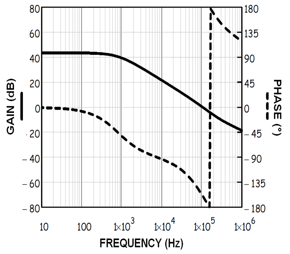
GVC(s) Bode Plot
Choose the crossover frequency with Equation 60.
Table 4. Calculated Compensation Network Components
| PARAMETER | CALCULATED VALUE | ACTUAL VALUE |
|---|---|---|
| RCOMP | 3.42 kΩ | 3.4 kΩ |
| CCOMP | 9.306 nF | 10 nF |
| CCOMP2 | 96.48 pF | 100 pF |
space
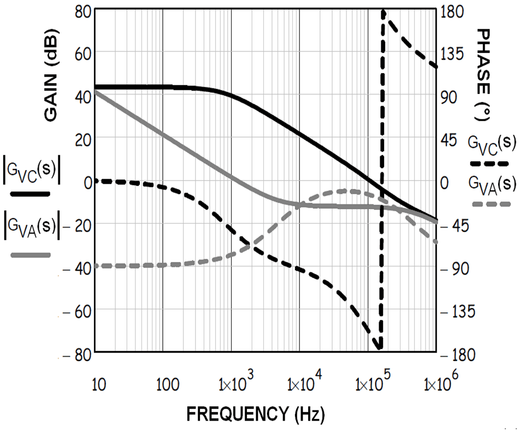
GVA(s) Bode Plots
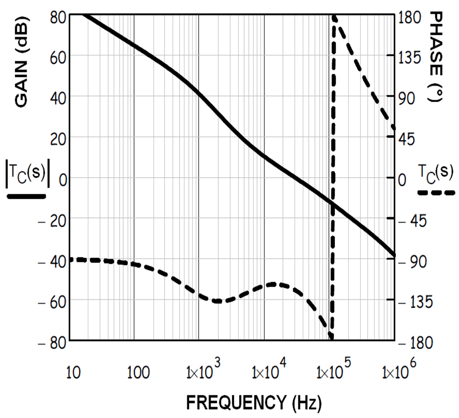
Table 5. Bill of Materials (BOM) for LM3017
| DESIGNATION | DESCRIPTION | SIZE | MANUFACTURER PART # | VENDOR |
|---|---|---|---|---|
| CIN1 | Cap 22 µF, 25 V X5R | 1206 | GRM31CR61E226KE15L | Murata |
| CO1,CO2, CO3 | Cap 22 µF, 25 V X5R | 1206 | GRM31CR61E226KE15L | Murata |
| CCOMP | Cap 0.022 µF | 0603 | C0603C103J1RACTU | Kemet |
| CCOMP2 | Cap 1000 pF | 0603 | C1608C0G1H101J | TDK |
| CBYP | Cap 0.1 µF, 25 V X7R | 0603 | 06033C104KAT2A | AVX |
| CVCC | Cap 0.47 µF, 16 V X7R | 0805 | C2012X7R1C474K | TDK |
| RCOMP | RES, 3.4 kΩ, 1%, 0.1W | 0603 | CRCW06033K40FKEA | Vishay |
| RFBT | RES, 21.5 kΩ, 1%, 0.1W | 0603 | CRCW060321K5FKEA | Vishay |
| RFBB | RES, 2 kΩ, 1%, 0.1W | 0603 | CRCW06032K00FKEA | Vishay |
| RS | RES, 100 Ω, 1%, 0.1W | 0603 | CRCW0603100RFKEA | Vishay |
| RSEN | RES, 0.03 Ω, 1%, 1W | 1206 | WSLP1206R0300FEA | Vishay |
| Q1 | NexFET™ N-CH, 25 V, 60 A, RDS(on)= 4.4 mΩ | 8-SON | CSD16323Q3 | TI |
| Q2 | NexFET™ N-CH, 25 V, 60 A, RDS(on)= 4.3 mΩ | 8-SON | CSD16340Q3 | TI |
| D1 | Diode Schottky, 30 V, 2 A | SMB | 20BQ030TRPBF | Vishay |
| L1 | Shielded Inductor, 4.7 µH, 2.3 A | 4 mm L × 4 mm W × 1.85 mm H | MPI4040R3-4R7-R | Cooper |
| U1 | LM3017 | — | — | TI |
8.2.3 Application Curve
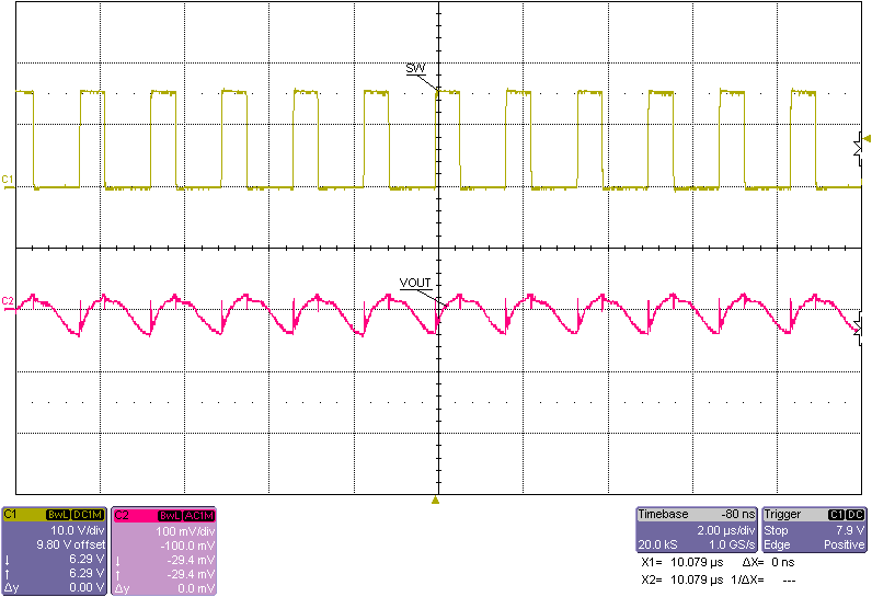 Figure 29. Switch Node and Output Voltage Ripple
With 5.5 VIN and 15 V at 1-A Output