SNOSC66D MARCH 2012 – September 2016 LM3017
PRODUCTION DATA.
- 1 Features
- 2 Applications
- 3 Description
- 4 Revision History
- 5 Pin Configuration and Functions
- 6 Specifications
- 7 Detailed Description
-
8 Application and Implementation
- 8.1 Application Information
- 8.2
Typical Application
- 8.2.1 Design Requirements
- 8.2.2
Detailed Design Procedure
- 8.2.2.1 Programming the Output Voltage
- 8.2.2.2 Power Inductor Selection
- 8.2.2.3 Setting the Output Current
- 8.2.2.4 Additional Slope Compensation
- 8.2.2.5 Current Limit With Additional Slope Compensation
- 8.2.2.6 Power Diode Selection
- 8.2.2.7 Low-Side MOSFET Selection (Switching MOSFET)
- 8.2.2.8 Pass MOSFET Selection (High-Side MOSFET)
- 8.2.2.9 Input Capacitor Selection
- 8.2.2.10 Output Capacitor Selection
- 8.2.2.11 VCC Decoupling Capacitor
- 8.2.2.12 Slope Compensation Ramp
- 8.2.2.13 Control Loop Compensation
- 8.2.3 Application Curve
- 9 Power Supply Recommendations
- 10Layout
- 11Device and Documentation Support
- 12Mechanical, Packaging, and Orderable Information
7 Detailed Description
7.1 Overview
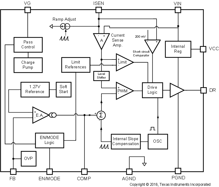
The LM3017 uses a fixed frequency, Pulse Width Modulated (PWM), current mode control architecture. A high-side current sense amplifier provides inductor current information by sensing the voltage drop across RSEN. The voltage across this resistor is fed into the ISEN pin. This voltage is then level shifted and fed into the positive input of the PWM comparator. As with all architectures of this type, a compensation ramp is required to ensure stability of the current control loop under all operating conditions. A nominal value of the ramp is provided internally while additional ramp can be added through the ISEN pin. The output voltage is sensed through an external feedback resistor divider network and fed into the error amplifier (EA) negative input (feedback pin, FB). The output of the error amplifier (COMP pin) is added to the slope compensation ramp and fed into the negative input of the PWM comparator.
At the start of any switching cycle, the oscillator sets a high signal on the DR pin (gate of the external MOSFET) and the external MOSFET turns on. When the voltage on the positive input of the PWM comparator exceeds the negative input, the Drive Logic is reset and the external MOSFET turns off.
Under extremely light load or no-load conditions, the energy delivered to the output capacitor when the external MOSFET is on during the minimum on time is more than what is delivered to the load. An overvoltage comparator inside the LM3017 prevents the output voltage from rising under these conditions by sensing the feedback (FB pin) voltage and resetting the RS latch. The latch remains in a reset state until the output decays to the nominal value. Thus the operating frequency decreases at light loads, resulting in excellent efficiency.
7.2 Functional Block Diagram

7.3 Feature Description
7.3.1 True Shutdown
The LM3017 incorporates circuitry to control a high side NMOS transistor in series with the inductor. This feature is used to disconnect the load from the input supply and protect the system from shorts on the output. Using an NMOS, rather than a PMOS transistor, saves the use of a diode from the inductor to ground. When the NMOS is turned off, the inductor brings the source belowground, keeping it on until the current is safely brought to zero. A built-in charge pump supplies typically VIN+ 5 V to drive the gate of this NMOS.
7.3.2 Operation of the EN/MODE Pin
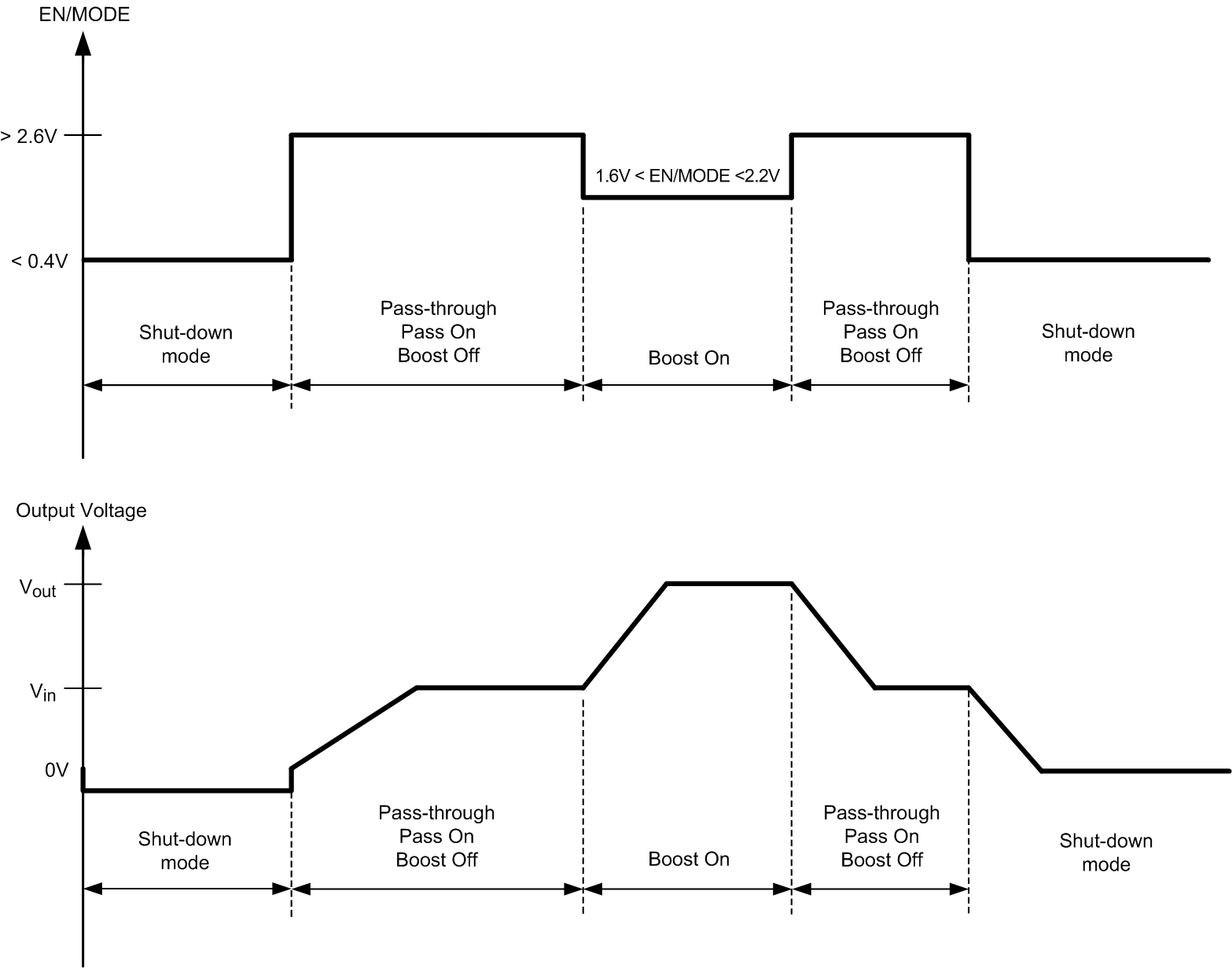
The EN/MODE pin is used to control the modes of the regulator by driving the high side gate (VG pin) to enable or disable the output through the pass MOSFET. Furthermore, it defines the current limit for each operation mode (see Device Functional Modes). Table 1 shows the modes versus the voltage on the EN/MODE pin.
Table 1. EN/MODE Voltage
| EN/MODE PIN VOLTAGE | MODE |
|---|---|
| ≤ 0.4 V | Shutdown |
| 1.6 V to 2.2 V | Boost |
| ≥ 2.6 V | Pass-through |
Figure 13 shows the output voltage behavior in the various operation modes.
7.3.3 EN/MODE Control
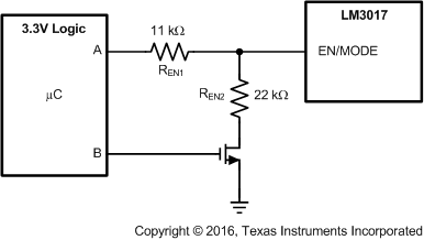
As stated previously, the EN/MODE pin controls the state of the LM3017. As with any digital input, the voltage on this pin must not be allowed to slowly cross the various thresholds. Although hysteresis is used on this input, slowly varying signal may cause unpredictable behavior. Also, the EN/MODE pin must not be allowed to float. One way to control the LM3017, from digital logic, is to use the circuit shown in Figure 14. The resistor values are adjusted based on the above table and the logic supply used. The MOSFET can be any small signal device, such as the 2N7002.
 Figure 13. Typical EN/MODE Operation
 Figure 14. Typical EN/MODE Control Circuit
7.3.4 Overvoltage Protection
The LM3017 incorporates output overvoltage protection (OVP). At light, or no load the minimum switch on-time may not be short enough to allow regulation in constant frequency PWM mode. In these cases, the output voltage (and therefore the voltage on the FB pin) tries to rise. When the voltage on the FB pin reaches approximately 20 mV higher than the regulation point, the power switch (Q1) is turned off. Q1 remains off until the FB voltage drops back to the regulation point, at which time normal switching begins again. In this way, the LM3017 prevents the output voltage from rising too high with no load on the output.
7.3.5 Thermal Protection
Internal thermal shutdown circuitry is provided to protect the LM3017 in the event that the maximum junction temperature is exceeded. When activated, typically at 165°C, the controller is forced into a low-power standby state, disabling the output driver and the VCC regulator. After the temperature is reduced (typical hysteresis is 10°C), the VCC regulator is re-enabled and the LM3017 performs a soft start.
7.3.6 Current Limit Protection
The LM3017 implements current limit protection by controlling the pass FET, Q2.
In boost mode the LM3017 features both cycle-by-cycle current limit and short-circuit protection. Unlike most boost regulators, the LM3017 can protect itself from short circuits on the output by shutting off the pass FET. The boost current limit, defined by VCL= 170 mV in Electrical Characteristics, turns off the boost FET for normal overloads on a cycle-by-cycle basis. The current is limited to VCL / RSEN until the overload is removed. If the output must be shorted, or otherwise pulled below VIN, the inductor current has a tendency to run-away. This is prevented by the short-circuit protection feature, defined as VSC = 200 mV in Electrical Characteristics. When this current limit is tripped, the current is limited to VSC / RSEN by controlling the pass FET. If the short persists for
TSC > 450 µs the pass FET is latched off. In this way, the current is limited to VSC / Rsen until the short is removed or the time of TSC = 450 µs is completed. Pulling the EN/MODE pin low (< 0.4 V, typical) is required to reset this short-circuit latch-off mode. The delay of TSC = 450 µs helps to prevent nuisance latch-off during a momentary short on the output.
7.4 Device Functional Modes
7.4.1 Shutdown Mode
Pulling the EN/MODE pin to less than 0.4 V (typical), during any mode of operation, places the part in full shutdown mode. The boost regulator and the pass FET is off and the load is disconnected from the input supply. In this mode, the regulator draws a maximum of 1 µA from the input supply.
7.4.2 Boost Mode
The boost regulator can be turned on by bringing the EN/MODE pin to greater than 1.6 V, but less than 2.2 V. This is the run mode for the boost regulator. Note that the LM3017 always starts in pass-through and transitions to boost mode.
7.4.3 Standby Mode
Setting the EN/MODE pin to greater than 2.6 V (typical), places the part in pass-through mode. The boost regulator is off and the pass MOSFET is on. During this mode, the load is connected to the input supply through the inductor and power diode, and is fully protected from output short circuits.
7.4.4 Start-Up Boost Mode
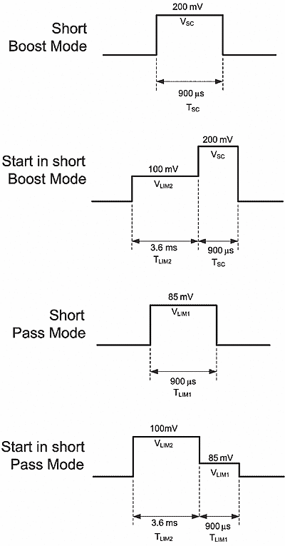
During start-up in boost mode, peak inductor current may be higher compared to normal operation. To allow for this, current limit levels and timing are different during start-up. The current limit is defined by VLIM2 = 100 mV (typical) in Electrical Characteristics, for the first TLIM2 = 3.6 ms (typical). The current is limited to VLIM2 / RSEN, for this period. Once the TLIM2 = 3.6 ms (typical) timer has finished, the current limit is increased to VSC = 200 mV (typical). For the first TLIM2 = 3.6 ms (typical) of the start-up, the latch-off feature is not enabled; however, the current is always limited to VLIM2 / RSEN. This allows the part to start up normally. If the current limit is still tripped at the end of TLIM2 = 3.6 ms (typical) , the TSC = 900 µs (typical) timer is started. Once the TSC = 900 µs (typical) time has expired, the pass FET (Q2) is latched off. This gives a total current-limited time of TSC + TLIM2 = 4.05 ms (typical), in cases where the LM3017 is started into a short circuit at the output.
7.4.5 Pass-Through Mode
In pass-through mode the power path is protected from shorts and overloads by the current limit defined as
VLIM1 = 85 mV (typical) in Electrical Characteristics. When this current limit is tripped, the current is limited to VLIM1 / RSEN by controlling the pass FET. If the short persists for TLIM1 > 900 µs (typical) the pass FET (Q2) is latched off. In this way, the current is limited to VLIM1 / RSEN until the short is removed or the time of
TLIM1 = 900 µs (typical) is completed. Pulling the EN/MODE pin low (0.4 V, typical) is required to reset this latch-off mode.
7.4.6 Start-Up Pass-Through Mode
During start-up in pass mode, the current limit is defined by VLIM2 = 100 mV (typical) in Electrical Characteristics, for the first TLIM2 = 3.6 ms (typical). The current is limited to VLIM2 / RSEN, for this period. Once the TLIM2 = 3.6 ms (typical) timer has finished, the current limit is reduced to VLIM1 = 85 mV (typical). For the first TLIM2 = 3.6 ms (typical) of the start-up, the latch-off feature is not enabled; however, the current is always limited to VLIM2 / RSEN. This higher limit allows the part to start up normally. If the current limit is still tripped at the end of TLIM2 = 3.6 ms (typical), the TLIM1 = 900 µs (typical) timer is started. Once the TLIM1= 900 µs time has expired, the pass FET(Q2) is latched off. This gives a total current-limited time of TLIM1+ TLIM2 = 4.5 ms (typical), in cases where the LM3017 is started into a short circuit at the output.
 Figure 15. Current Limit and Short-Circuit Protection