SNOSC66D MARCH 2012 – September 2016 LM3017
PRODUCTION DATA.
- 1 Features
- 2 Applications
- 3 Description
- 4 Revision History
- 5 Pin Configuration and Functions
- 6 Specifications
- 7 Detailed Description
-
8 Application and Implementation
- 8.1 Application Information
- 8.2
Typical Application
- 8.2.1 Design Requirements
- 8.2.2
Detailed Design Procedure
- 8.2.2.1 Programming the Output Voltage
- 8.2.2.2 Power Inductor Selection
- 8.2.2.3 Setting the Output Current
- 8.2.2.4 Additional Slope Compensation
- 8.2.2.5 Current Limit With Additional Slope Compensation
- 8.2.2.6 Power Diode Selection
- 8.2.2.7 Low-Side MOSFET Selection (Switching MOSFET)
- 8.2.2.8 Pass MOSFET Selection (High-Side MOSFET)
- 8.2.2.9 Input Capacitor Selection
- 8.2.2.10 Output Capacitor Selection
- 8.2.2.11 VCC Decoupling Capacitor
- 8.2.2.12 Slope Compensation Ramp
- 8.2.2.13 Control Loop Compensation
- 8.2.3 Application Curve
- 9 Power Supply Recommendations
- 10Layout
- 11Device and Documentation Support
- 12Mechanical, Packaging, and Orderable Information
10 Layout
10.1 Layout Guidelines
Good board layout is critical for switching controllers such as the LM3017. First the ground plane area must be sufficient for thermal dissipation purposes and second, appropriate guidelines must be followed to reduce the effects of switching noise. Switch mode converters are very fast switching devices. In such devices, the rapid increase of input current combined with the parasitic trace inductance generates unwanted voltage noise spikes. The magnitude of this noise tends to increase as the output current increases. This parasitic spike noise may create electromagnetic interference (EMI), and can also cause problems in device performance. Therefore, take care in layout to minimize the effect of this switching noise.
10.1.1 Filter Capacitors
Ceramic filter capacitors are most effective when the inductance of the current loops that they filter is minimized. Place CBYP as close as possible to the VIN and GND pins of the LM3017. Place CVCC next to the VCC and GND pins of the LM3017 (see Figure 16 for designators).
10.1.2 Sense Lines
The current sensing circuit in current mode devices can be easily effected by switching noise. This noise can cause duty cycle jitter which leads to increased spectral noise. RSEN must be connected to the ISEN pin with a separate trace made as short as possible, TI also recommends to route the trace that connects the VIN pin to the input voltage as close as possible to RSEN. Route this trace away from the inductor and the switch node (where D1, Q1, and L1 connect). For the voltage loop, keep RFBB/T close to the LM3017 and run a trace as close as possible to the positive side of CO. As with the ISEN line, the FB line must be routed away from the inductor and the switch node. These measures minimize the length of high impedance lines and reduce noise pickup.
10.1.3 Compact Layout
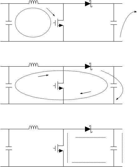
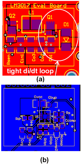
The most important layout rule is to keep the AC current loops as small as possible. Figure 30 shows the current flow of a boost converter. The top schematic shows a dotted line which represents the current flow during on-state and the middle schematic shows the current flow during off-state. The bottom schematic shows the currents referred to as AC currents. They are the most critical ones because current is changing in very short time periods. The dotted line traces of the bottom schematic are the ones to make as short as possible. In a boost regulator the primary switching loop consists of the output capacitor, diode and MOSFET. Minimizing the area of this loop reduces the stray inductances and minimizes noise and possible erratic operation (see Layout Examples). The output capacitor(s) must be placed as close as possible to the diode cathode and MOSFET GND.
 Figure 30. Current Flow in a Boost Application
10.1.4 Ground Plane and Vias
A ground plane in the printed-circuit board is recommended as a means to connect the quiet end (input voltage ground side) of the input filter capacitor to the output filter capacitors and the PGND pin of the controller. Connect all the low power ground connections directly to the regulator AGND. Connect the AGND and PGND pins together through a copper area covering the entire underside of the device. Place several vias in this underside copper area to ground plane. If a via is required to connect the sensing resistor to the ISEN pin, then place that via in the inner side of the sensing resistor such that no current flow occurs. Place several vias from the ground side of the output capacitor(s) to ground place, that minimizes the path for AC current. The PGND and AGND pins have to be connected to the same ground very close to the IC. To avoid ground loop currents attach all the grounds of the system only at one point.
10.2 Layout Examples
 Figure 31. Layout Example (a) Top Layer, (b) Bottom Layer
10.3 Thermal Considerations
The majority of power dissipation and heat generation comes from FETs and diode. Selecting MOSFETs with exposed pads aids the power dissipation of these devices. Careful attention to RDS(on) at high temperature must be observed. Diode data sheets provide a typical junction-to-ambient thermal resistance RθJA, which can be used to estimate the operating die temperature of the Schottky. Multiplying the power dissipation by RθJA gives the temperature rise. The diode case size can then be selected to maintain the Schottky diode temperature below the operational maximum. Larger case sizes generally have lower RθJA and lower forward voltage drop.