SNVS118F december   1999  – may 2023 LM2594 , LM2594HV

PRODUCTION DATA  

  1.   1
  2. Features
  3. Applications
  4. Description
  5. Revision History
  6. Description (continued)
  7. Pin Configuration and Functions
  8. Specifications
    1. 7.1  Absolute Maximum Ratings
    2. 7.2  ESD Ratings
    3. 7.3  Recommended Operating Conditions
    4. 7.4  Thermal Information
    5. 7.5  Electrical Characteristics – 3.3 V
    6. 7.6  Electrical Characteristics – 5 V
    7. 7.7  Electrical Characteristics – 12 V
    8. 7.8  Electrical Characteristics – Adjustable
    9. 7.9  Electrical Characteristics – All Output Voltage Versions
    10. 7.10 Typical Characteristics
  9. Detailed Description
    1. 8.1 Overview
    2. 8.2 Functional Block Diagram
    3. 8.3 Feature Description
      1. 8.3.1 Delayed Start-Up
      2. 8.3.2 Undervoltage Lockout
      3. 8.3.3 Inverting Regulator
      4. 8.3.4 Inverting Regulator Shutdown Methods
    4. 8.4 Device Functional Modes
      1. 8.4.1 Discontinuous Mode Operation
  10. Application and Implementation
    1. 9.1 Application Information
      1. 9.1.1 Input Capacitor (CIN)
      2. 9.1.2 Output Capacitor (COUT)
      3. 9.1.3 Catch Diode
      4. 9.1.4 Inductor Selection
      5. 9.1.5 Output Voltage Ripple and Transients
      6. 9.1.6 Open Core Inductors
    2. 9.2 Typical Applications
      1. 9.2.1 Series Buck Regulator (Fixed Output)
        1. 9.2.1.1 Design Requirements
        2. 9.2.1.2 Detailed Design Procedure
          1. 9.2.1.2.1 Custom Design with WEBENCH® Tools
          2. 9.2.1.2.2 Inductor Selection (L1)
          3. 9.2.1.2.3 Output Capacitor Selection (COUT)
          4. 9.2.1.2.4 Catch Diode Selection (D1)
          5. 9.2.1.2.5 Input Capacitor (CIN)
        3. 9.2.1.3 Application Curves
      2. 9.2.2 Series Buck Regulator (Adjustable Output)
        1. 9.2.2.1 Design Requirements
        2. 9.2.2.2 Detailed Design Procedure
          1. 9.2.2.2.1 Programming Output Voltage
          2. 9.2.2.2.2 Inductor Selection (L1)
          3. 9.2.2.2.3 Output Capacitor Selection (COUT)
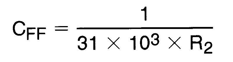
          4. 9.2.2.2.4 Feedforward Capacitor (CFF)
          5. 9.2.2.2.5 Catch Diode Selection (D1)
          6. 9.2.2.2.6 Input Capacitor (CIN)
        3. 9.2.2.3 Application Curves
    3. 9.3 Power Supply Recommendations
    4. 9.4 Layout
      1. 9.4.1 Layout Guidelines
      2. 9.4.2 Layout Example
      3. 9.4.3 Thermal Considerations
  11. 10Device and Documentation Support
    1. 10.1 Device Support
      1. 10.1.1 Development Support
        1. 10.1.1.1 Custom Design with WEBENCH® Tools
    2. 10.2 Receiving Notification of Documentation Updates
    3. 10.3 Support Resources
    4. 10.4 Trademarks
    5. 10.5 Electrostatic Discharge Caution
    6. 10.6 Glossary
  12. 11Mechanical, Packaging, and Orderable Information

封装选项

机械数据 (封装 | 引脚)
散热焊盘机械数据 (封装 | 引脚)
订购信息
Feedforward Capacitor (CFF)

For output voltages greater than approximately 10 V, an additional capacitor is required. The compensation capacitor is typically between 50 pF and 10 nF, and is wired in parallel with the output voltage setting resistor, R2. It provides additional stability for high output voltages, low input or output voltages, and very low ESR output capacitors, such as solid tantalum capacitors calculated with Equation 7.

Equation 7. GUID-AE4EC551-9648-474D-B421-A3E59B5B1F51-low.png

This capacitor type can be ceramic, plastic, silver mica, and so forth (because of the unstable characteristics of ceramic capacitors made with Z5U material, they are not recommended).

Table 9-7 contains feedforward capacitor values for various output voltages. In this example, a 1-nF capacitor is needed.