SNVS118F december   1999  – may 2023 LM2594 , LM2594HV

PRODUCTION DATA  

  1.   1
  2. Features
  3. Applications
  4. Description
  5. Revision History
  6. Description (continued)
  7. Pin Configuration and Functions
  8. Specifications
    1. 7.1  Absolute Maximum Ratings
    2. 7.2  ESD Ratings
    3. 7.3  Recommended Operating Conditions
    4. 7.4  Thermal Information
    5. 7.5  Electrical Characteristics – 3.3 V
    6. 7.6  Electrical Characteristics – 5 V
    7. 7.7  Electrical Characteristics – 12 V
    8. 7.8  Electrical Characteristics – Adjustable
    9. 7.9  Electrical Characteristics – All Output Voltage Versions
    10. 7.10 Typical Characteristics
  9. Detailed Description
    1. 8.1 Overview
    2. 8.2 Functional Block Diagram
    3. 8.3 Feature Description
      1. 8.3.1 Delayed Start-Up
      2. 8.3.2 Undervoltage Lockout
      3. 8.3.3 Inverting Regulator
      4. 8.3.4 Inverting Regulator Shutdown Methods
    4. 8.4 Device Functional Modes
      1. 8.4.1 Discontinuous Mode Operation
  10. Application and Implementation
    1. 9.1 Application Information
      1. 9.1.1 Input Capacitor (CIN)
      2. 9.1.2 Output Capacitor (COUT)
      3. 9.1.3 Catch Diode
      4. 9.1.4 Inductor Selection
      5. 9.1.5 Output Voltage Ripple and Transients
      6. 9.1.6 Open Core Inductors
    2. 9.2 Typical Applications
      1. 9.2.1 Series Buck Regulator (Fixed Output)
        1. 9.2.1.1 Design Requirements
        2. 9.2.1.2 Detailed Design Procedure
          1. 9.2.1.2.1 Custom Design with WEBENCH® Tools
          2. 9.2.1.2.2 Inductor Selection (L1)
          3. 9.2.1.2.3 Output Capacitor Selection (COUT)
          4. 9.2.1.2.4 Catch Diode Selection (D1)
          5. 9.2.1.2.5 Input Capacitor (CIN)
        3. 9.2.1.3 Application Curves
      2. 9.2.2 Series Buck Regulator (Adjustable Output)
        1. 9.2.2.1 Design Requirements
        2. 9.2.2.2 Detailed Design Procedure
          1. 9.2.2.2.1 Programming Output Voltage
          2. 9.2.2.2.2 Inductor Selection (L1)
          3. 9.2.2.2.3 Output Capacitor Selection (COUT)
          4. 9.2.2.2.4 Feedforward Capacitor (CFF)
          5. 9.2.2.2.5 Catch Diode Selection (D1)
          6. 9.2.2.2.6 Input Capacitor (CIN)
        3. 9.2.2.3 Application Curves
    3. 9.3 Power Supply Recommendations
    4. 9.4 Layout
      1. 9.4.1 Layout Guidelines
      2. 9.4.2 Layout Example
      3. 9.4.3 Thermal Considerations
  11. 10Device and Documentation Support
    1. 10.1 Device Support
      1. 10.1.1 Development Support
        1. 10.1.1.1 Custom Design with WEBENCH® Tools
    2. 10.2 Receiving Notification of Documentation Updates
    3. 10.3 Support Resources
    4. 10.4 Trademarks
    5. 10.5 Electrostatic Discharge Caution
    6. 10.6 Glossary
  12. 11Mechanical, Packaging, and Orderable Information

封装选项

机械数据 (封装 | 引脚)
散热焊盘机械数据 (封装 | 引脚)
订购信息

Delayed Start-Up

The circuit in Figure 8-1 uses the ON/OFF pin to provide a time delay between the time the input voltage is applied and the time the output voltage comes up (only the circuitry pertaining to the delayed start-up is shown). As the input voltage rises, the charging of capacitor C1 pulls the ON/OFF pin high, keeping the regulator off. After the input voltage reaches its final value and the capacitor stops charging, the resistor R2 pulls the ON/OFF pin low, thus allowing the circuit to start switching. Resistor R1 is included to limit the maximum voltage applied to the ON/OFF pin (maximum of 25 V), reduces power supply noise sensitivity, and also limits the capacitor, C1, discharge current. When high input ripple voltage exists, avoid long delay time, because this ripple can be coupled into the ON/OFF pin and cause problems.

This delayed start-up feature is useful in situations where the input power source is limited in the amount of current it can deliver. It allows the input voltage to rise to a higher voltage before the regulator starts operating. Buck regulators require less input current at higher input voltages.
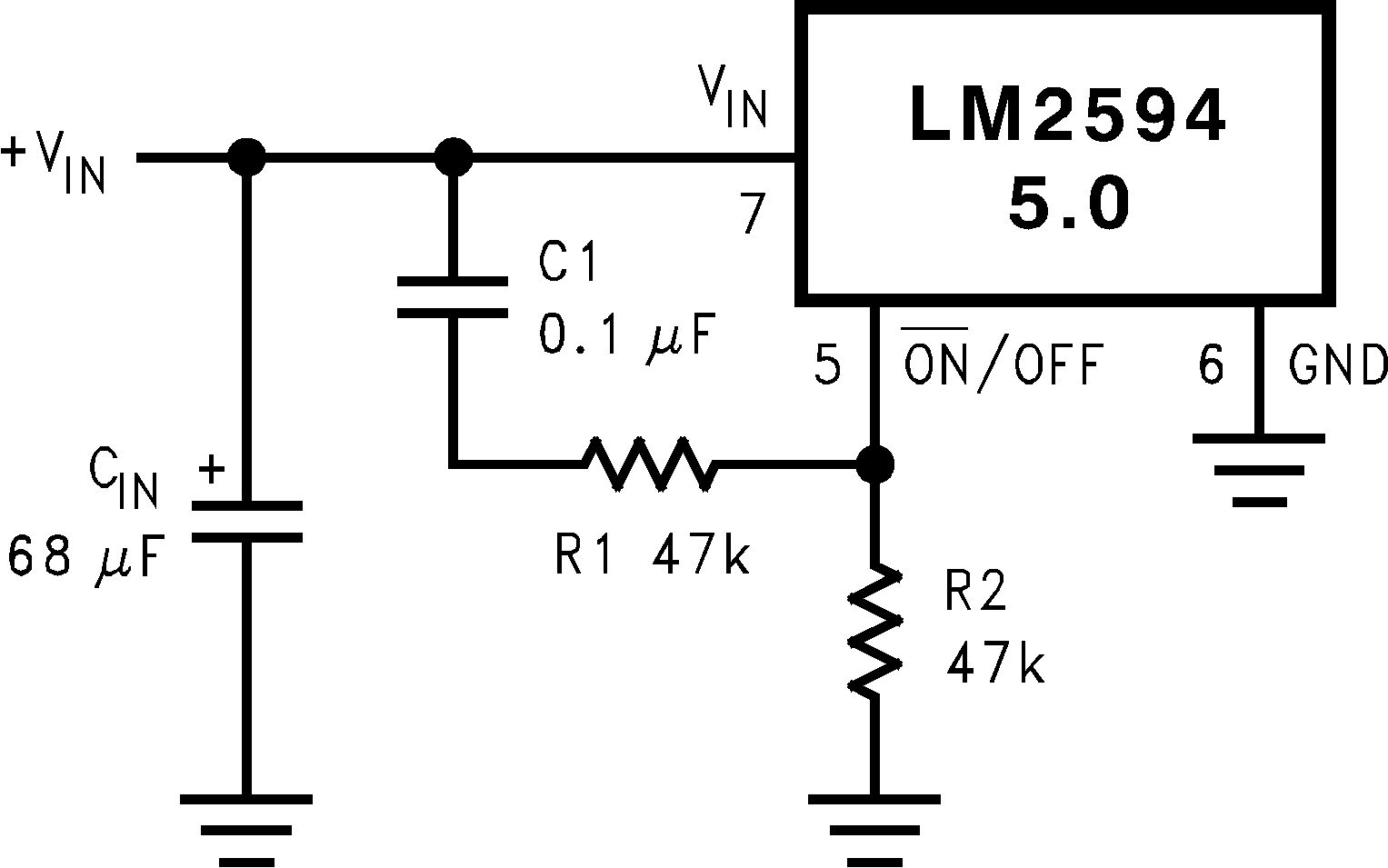
GUID-EBEB9126-786E-45D3-9669-E68EA8BD2B35-low.pngFigure 8-1 Delayed Start-Up