SLUS696C June   2006  – February 2019

PRODUCTION DATA.  

  1. Features
  2. Applications
  3. Description
    1.     Device Images
      1.      Simplified Schematic
  4. Revision History
  5. Pin Configuration and Functions
    1.     Pin Functions
  6. Specifications
    1. 6.1 Absolute Maximum Ratings
    2. 6.2 ESD Ratings
    3. 6.3 Recommended Operating Conditions
    4. 6.4 Thermal Information
    5. 6.5 Electrical Characteristics
    6. 6.6 Standard Serial Communication (SDQ) Timing
    7. 6.7 OTP Programming Specifications
    8. 6.8 Typical Characteristics
  7. Detailed Description
    1. 7.1 Overview
    2. 7.2 Functional Block Diagram
    3. 7.3 Feature Description
      1. 7.3.1 Non-Volatile Memory
      2. 7.3.2 Authentication
      3. 7.3.3 Communication and Power
    4. 7.4 Device Functional Modes
      1. 7.4.1 Profile Command
      2. 7.4.2 Sleep Mode Description
    5. 7.5 Programming
      1. 7.5.1 Communicating with the bq26100 Device
      2. 7.5.2 Memory Descriptions
        1. 7.5.2.1 Non-Volatile OTP Memory
          1. 7.5.2.1.1 General Use – Memory Function Commands 0xF0 (Read) and 0x0F (Write)
          2. 7.5.2.1.2 General Use — Memory Function Commands 0xFA (Read) and 0xAF (Write)
          3. 7.5.2.1.3 Status – Memory Function Commands 0xAA (Read) and 0x55 (Write)
            1. 7.5.2.1.3.1 PAGE LOCK (offset = D431h) [reset = 0h]
              1. Table 5. PAGE LOCK Field Descriptions
        2. 7.5.2.2 Non-Volatile EEPROM Memory
          1. 7.5.2.2.1 General Use – Memory Function Commands 0xE0 (Read) and 0x0E (Write)
      3. 7.5.3 SHA-1 Description
      4. 7.5.4 Key Programming Description
    6. 7.6 Register Maps
      1. 7.6.1 Volatile Register Memory
        1. 7.6.1.1 Message and Digest Registers – Memory Function Command 0xDD (Read) and 0x22 (Write)
        2. 7.6.1.2 Control and Version Registers – Memory Function Command 0x88 (Read) and 0x77 (Write)
          1. 7.6.1.2.1 CTRL Register (address = 0001h) [reset = 1h]
            1. Table 9. Control Register Field Descriptions
  8. Application and Implementation
    1. 8.1 Application Information
    2. 8.2 Typical Application
      1. 8.2.1 Design Requirements
      2. 8.2.2 Detailed Design Procedure
  9. Power Supply Recommendations
  10. 10Layout
    1. 10.1 Layout Guidelines
    2. 10.2 Layout Example
  11. 11Device and Documentation Support
    1. 11.1 Receiving Notification of Documentation Updates
    2. 11.2 Community Resources
    3. 11.3 Trademarks
    4. 11.4 Electrostatic Discharge Caution
    5. 11.5 Glossary
  12. 12Mechanical, Packaging, and Orderable Information

封装选项

机械数据 (封装 | 引脚)
散热焊盘机械数据 (封装 | 引脚)
订购信息

Key Programming Description

The 128-bit key used in the HMAC calculation is built from two 64-bit key spaces on the bq26100 device. Each key can be programmed independently, allowing multiple parties to program part of the full 128-bit key without the knowledge necessary to reproduce the full 128-bit key. To further protect the 128-bit key, the value written to each 64-bit non-volatile key space is the output of a SHA-1 calculation on a 160-bit input. Figure 18 provides a flow for the programming of the 128-bit device key. Once KEYx has been programmed, the LOCKKx bit should be programmed to 0 in the status register, preventing another value from overwriting that key space.
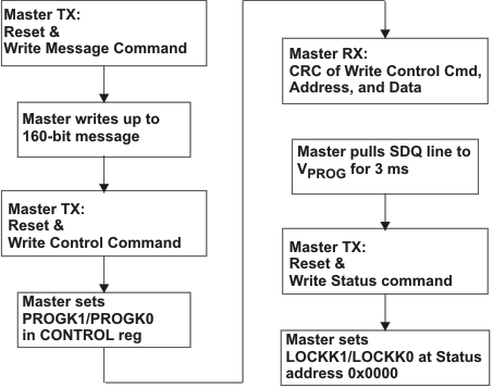
bq26100 key_prog_lus696.gifFigure 18. Key Programming Flow

This flow is run twice, for KEY0 and KEY1. An external power source is required on the PWR pin during key programming. Figure 20 shows a typical connection for the external power source.

Since there is no key pre-appended to the message, the key message is padded with a 1, followed by 287 0’s, followed by the 64-bit value for 160 (00..01010000), see Figure 19.

bq26100 sha1_2_blk_lus696.gifFigure 19. Key Programming Message Format Example
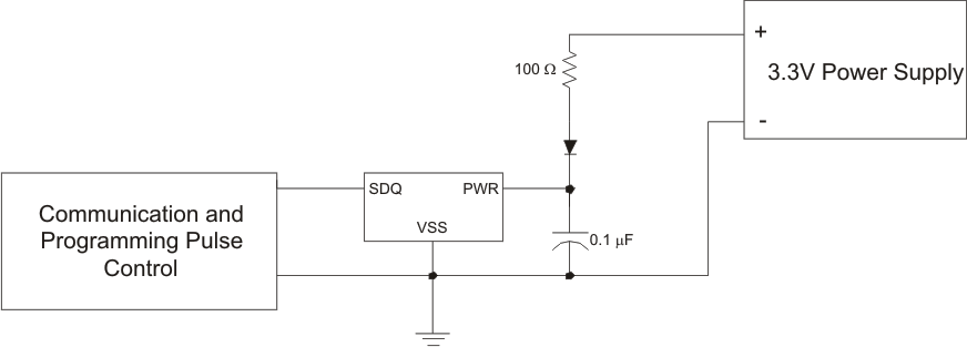
bq26100 keypgm_lus696.gifFigure 20. External Power Source Connection