SLUS696C June   2006  – February 2019

PRODUCTION DATA.  

  1. Features
  2. Applications
  3. Description
    1.     Device Images
      1.      Simplified Schematic
  4. Revision History
  5. Pin Configuration and Functions
    1.     Pin Functions
  6. Specifications
    1. 6.1 Absolute Maximum Ratings
    2. 6.2 ESD Ratings
    3. 6.3 Recommended Operating Conditions
    4. 6.4 Thermal Information
    5. 6.5 Electrical Characteristics
    6. 6.6 Standard Serial Communication (SDQ) Timing
    7. 6.7 OTP Programming Specifications
    8. 6.8 Typical Characteristics
  7. Detailed Description
    1. 7.1 Overview
    2. 7.2 Functional Block Diagram
    3. 7.3 Feature Description
      1. 7.3.1 Non-Volatile Memory
      2. 7.3.2 Authentication
      3. 7.3.3 Communication and Power
    4. 7.4 Device Functional Modes
      1. 7.4.1 Profile Command
      2. 7.4.2 Sleep Mode Description
    5. 7.5 Programming
      1. 7.5.1 Communicating with the bq26100 Device
      2. 7.5.2 Memory Descriptions
        1. 7.5.2.1 Non-Volatile OTP Memory
          1. 7.5.2.1.1 General Use – Memory Function Commands 0xF0 (Read) and 0x0F (Write)
          2. 7.5.2.1.2 General Use — Memory Function Commands 0xFA (Read) and 0xAF (Write)
          3. 7.5.2.1.3 Status – Memory Function Commands 0xAA (Read) and 0x55 (Write)
            1. 7.5.2.1.3.1 PAGE LOCK (offset = D431h) [reset = 0h]
              1. Table 5. PAGE LOCK Field Descriptions
        2. 7.5.2.2 Non-Volatile EEPROM Memory
          1. 7.5.2.2.1 General Use – Memory Function Commands 0xE0 (Read) and 0x0E (Write)
      3. 7.5.3 SHA-1 Description
      4. 7.5.4 Key Programming Description
    6. 7.6 Register Maps
      1. 7.6.1 Volatile Register Memory
        1. 7.6.1.1 Message and Digest Registers – Memory Function Command 0xDD (Read) and 0x22 (Write)
        2. 7.6.1.2 Control and Version Registers – Memory Function Command 0x88 (Read) and 0x77 (Write)
          1. 7.6.1.2.1 CTRL Register (address = 0001h) [reset = 1h]
            1. Table 9. Control Register Field Descriptions
  8. Application and Implementation
    1. 8.1 Application Information
    2. 8.2 Typical Application
      1. 8.2.1 Design Requirements
      2. 8.2.2 Detailed Design Procedure
  9. Power Supply Recommendations
  10. 10Layout
    1. 10.1 Layout Guidelines
    2. 10.2 Layout Example
  11. 11Device and Documentation Support
    1. 11.1 Receiving Notification of Documentation Updates
    2. 11.2 Community Resources
    3. 11.3 Trademarks
    4. 11.4 Electrostatic Discharge Caution
    5. 11.5 Glossary
  12. 12Mechanical, Packaging, and Orderable Information

封装选项

机械数据 (封装 | 引脚)
散热焊盘机械数据 (封装 | 引脚)
订购信息

Detailed Design Procedure

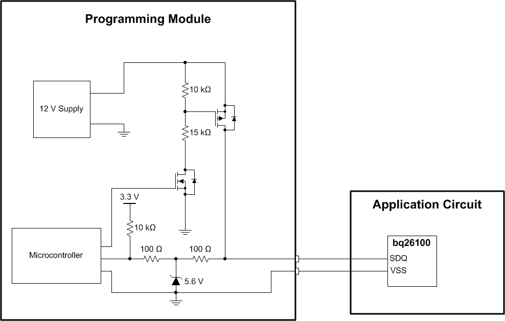
The bq26100 device requires a 12-V maximum-pulse signal to program the OTP memory. It is necessary to have a programming test setup for production. shows an example of what the circuit could be for such a setup. The Programming Module contains the microcontroller that acts as SDQ master and also controls the time of the programming pulse and its width. The 12-V supply is the source for the programming pulse. Only SDQ and VSS signals need to exit the test setup as the Application Circuit containing the bq26100 device under test is connected only for programming and verifying data.

The Programming Module typically will connect to a PC using an interface such as USB. The diagram in does not include the interface to a PC, which can vary depending on the system designer's choice.
bq26100 lus696_progCircuitApp.gifFigure 25. Programming Circuit Example