ZHCSIU4A September   2018  – August 2019 ADS1284

PRODUCTION DATA.  

  1. 特性
  2. 应用
  3. 说明
    1.     Device Images
      1.      简化原理图
  4. 修订历史记录
  5. Pin Configuration and Functions
    1.     Pin Functions
  6. Specifications
    1. 6.1 Absolute Maximum Ratings
    2. 6.2 ESD Ratings
    3. 6.3 Recommended Operating Conditions
    4. 6.4 Thermal Information
    5. 6.5 Electrical Characteristics
    6. 6.6 Timing Requirements
    7. 6.7 Switching Characteristics
    8. 6.8 Typical Characteristics
  7. Parameter Measurement Information
    1. 7.1 Noise Performance
  8. Detailed Description
    1. 8.1 Overview
    2. 8.2 Functional Block Diagram
    3. 8.3 Feature Description
      1. 8.3.1 Analog Inputs and Multiplexer
      2. 8.3.2 Programmable Gain Amplifier (PGA)
      3. 8.3.3 Analog-to-Digital Converter (ADC)
        1. 8.3.3.1 Modulator
          1. 8.3.3.1.1 Modulator Overrange
          2. 8.3.3.1.2 Modulator Input Impedance
          3. 8.3.3.1.3 Modulator Overrange Detection (MFLAG)
          4. 8.3.3.1.4 Offset
          5. 8.3.3.1.5 Voltage Reference Inputs (VREFP, VREFN)
        2. 8.3.3.2 Digital Filter
          1. 8.3.3.2.1 Sinc Filter Section (sinx / x)
          2. 8.3.3.2.2 FIR Section
          3. 8.3.3.2.3 Group Delay and Step Response
            1. 8.3.3.2.3.1 Linear Phase Response
            2. 8.3.3.2.3.2 Minimum Phase Response
          4. 8.3.3.2.4 HPF Section
    4. 8.4 Device Functional Modes
      1. 8.4.1  Synchronization (SYNC PIN and SYNC Command)
        1. 8.4.1.1 Pulse-Sync Mode
        2. 8.4.1.2 Continuous-Sync Mode
      2. 8.4.2  Reset (RESET Pin and Reset Command)
      3. 8.4.3  Master Clock Input (CLK)
      4. 8.4.4  Power-Down (PWDN Pin and STANDBY Command)
      5. 8.4.5  Power-On Sequence
      6. 8.4.6  DVDD Power Supply
      7. 8.4.7  Serial Interface
        1. 8.4.7.1 Chip Select (CS)
        2. 8.4.7.2 Serial Clock (SCLK)
        3. 8.4.7.3 Data Input (DIN)
        4. 8.4.7.4 Data Output (DOUT)
        5. 8.4.7.5 Serial Port Auto Timeout
        6. 8.4.7.6 Data Ready (DRDY)
      8. 8.4.8  Data Format
      9. 8.4.9  Reading Data
        1. 8.4.9.1 Read-Data-Continuous Mode
        2. 8.4.9.2 Read-Data-By-Command Mode
      10. 8.4.10 One-Shot Operation
      11. 8.4.11 Offset and Full-Scale Calibration Registers
        1. 8.4.11.1 OFC[2:0] Registers
        2. 8.4.11.2 FSC[2:0] Registers
      12. 8.4.12 Calibration Commands (OFSCAL and GANCAL)
        1. 8.4.12.1 OFSCAL Command
        2. 8.4.12.2 GANCAL Command
      13. 8.4.13 User Calibration
    5. 8.5 Programming
      1. 8.5.1 Commands
        1. 8.5.1.1  SDATAC Requirements
        2. 8.5.1.2  WAKEUP: Wake-Up From Standby Mode
        3. 8.5.1.3  STANDBY: Standby Mode
        4. 8.5.1.4  SYNC: Synchronize the Analog-to-Digital Conversion
        5. 8.5.1.5  RESET: Reset the Device
        6. 8.5.1.6  RDATAC: Read Data Continuous
        7. 8.5.1.7  SDATAC: Stop Read Data Continuous
        8. 8.5.1.8  RDATA: Read Data by Command
        9. 8.5.1.9  RREG: Read Register Data
        10. 8.5.1.10 WREG: Write to Register
        11. 8.5.1.11 OFSCAL: Offset Calibration
        12. 8.5.1.12 GANCAL: Gain Calibration
    6. 8.6 Register Maps
      1. 8.6.1 Register Descriptions
        1. 8.6.1.1 ID_CFG: ID_Configuration Register (address = 00h) [reset =x0h]
        2. 8.6.1.2 CONFIG0: Configuration Register 0 (address = 01h) [reset = 52h]
        3. 8.6.1.3 CONFIG1: Configuration Register 1 (address = 02h) [reset = 08h]
        4. 8.6.1.4 HPF0 and HPF1 Registers
          1. 8.6.1.4.1 HPF0: High-Pass Filter Corner Frequency, Low Byte (address = 03h) [reset = 32h]
          2. 8.6.1.4.2 HPF1: High-Pass Filter Corner Frequency, High Byte (address = 04h) [reset = 03h]
        5. 8.6.1.5 OFC0, OFC1, OFC2 Registers
          1. 8.6.1.5.1 OFC0: Offset Calibration, Low Byte (address = 05h) [reset = 00h]
          2. 8.6.1.5.2 OFC1: Offset Calibration, Mid Byte (address = 06h) [reset = 00h]
          3. 8.6.1.5.3 OFC2: Offset Calibration, High Byte (address = 07h) [reset = 00h]
        6. 8.6.1.6 FSC0, FSC1, FSC2 Registers
          1. 8.6.1.6.1 FSC0: Full-Scale Calibration, Low Byte (address = 08h) [reset = 00h]
          2. 8.6.1.6.2 FSC1: Full-Scale Calibration, Mid Byte (address = 09h) [reset = 00h]
          3. 8.6.1.6.3 FSC2: Full-Scale Calibration, High Byte (address = 0Ah) [reset = 40h]
  9. Application and Implementation
    1. 9.1 Application Information
    2. 9.2 Typical Applications
      1. 9.2.1 Geophone Interface
      2. 9.2.2 Digital Interface
    3. 9.3 Initialization Set Up
  10. 10器件和文档支持
    1. 10.1 接收文档更新通知
    2. 10.2 社区资源
    3. 10.3 商标
    4. 10.4 静电放电警告
    5. 10.5 Glossary
  11. 11机械、封装和可订购信息

封装选项

机械数据 (封装 | 引脚)
散热焊盘机械数据 (封装 | 引脚)
订购信息

Modulator

The low-noise modulator is an inherently-stable, fourth-order, ΔΣ, 2 + 2 pipelined structure, as Figure 38 shows. The modulator shifts the quantization noise to a higher frequency (out of the passband), where the noise is removed by the digital filter. The modulator data can either be completely filtered by the on-chip digital filter or partially filtered by use of the sinc filter section alone. Partial filtering provided by the sinc filter section is intended for use with an external FIR filter.
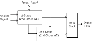
ADS1284 ai_mod_4order_bas565.gifFigure 38. ADS1284 Fourth-Order Modulator

Modulator performance is optimized for input signal frequencies over the range dc to 2 kHz. As Figure 39 shows, the effect of PGA and modulator chop result in spectral artifacts occurring at the chop frequency (4 kHz) and harmonics related of the chop frequency. When using the sinc filter output in conjunction with an external post-decimation filter, design the external filter to suppress the modulator chopping artifacts.
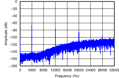
ADS1284 C001_SBAS565.pngFigure 39. Sinc Output FFT (64 kSPS)