ZHCU772 December 2021
- 说明
- 资源
- 特性
- 应用
- 5
- 1System Overview
- 2Hardware, Software, Testing Requirements, and Test Results
- 3Design and Documentation Support
- 4About the Author
- 5Acknowledgement
2.1.1.5 Hardware Setup of Multiple Transceiver Synchronization
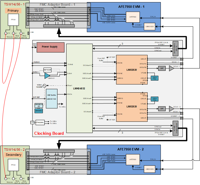
The proposed LMX2820 clocking solution is interfaced with two AFE7950EVMs and two TSW14J56EVM capture cards to show the synchronization between multiple AFE7950 devices. Figure 2-2 shows the overall block diagram of the multiple transceiver synchronized system.
 Figure 2-2 TIDA-010230 Device
Synchronization Block Diagram
Figure 2-2 TIDA-010230 Device
Synchronization Block DiagramTable 2-1 shows the AFE7950 operating modes and frequency requirements for various tests in this design.
| Parameters \ Test | TX Performance | RX Performance | Synchronization Test |
|---|---|---|---|
| Transmitter Mode | 44210 | - | 44210 |
| Interpolation | 18 | - | 18 |
| DAC Sampling Frequency (MHz) | 8847.36 | - | 8847.36 |
| Interpolated DAC clock rate (MHz) | 491.52 | - | 491.52 |
| K | 16 | - | 16 |
| F | 2 | - | 2 |
| Lane rate (Mbps) | 9830.4 | - | 9830.4 |
| Receiver Mode | - | 44210 | 24410 |
| Decimation | - | 6 | 12 |
| ADC Sampling Frequency (MHz) | - | 2949.12 | 2949.12 |
| Decimated output rate (MHz) | - | 491.52 | 245.76 |
| K | - | 16 | 32 |
| F | - | 2 | 4 |
| Lane rate (Mbps) | - | 9830.4 | 9830.4 |
| SYSREF Frequency (MHz) | 1.92 | 1.92 | 1.92 |
| FPGA Clock (MHz) | 245.76 | 245.76 | 245.76 |
The AFE7950EVM was tested with the proposed LMX2820 clocking solution for various test cases and modes to see the transmitter and receiver performance and compare with the data sheet performance along with a synchronization test for common frequency settings.