ZHCU740 April   2020


  1.    说明
  2.    资源
  3.    特性
  4.    应用
  5.    设计图像
  6. 1System Overview
    1. 1.1 Key System Specifications
    2. 1.2 Block Diagram
    3. 1.3 Top Side Pump
    4. 1.4 LED Driver Input Signals
    5. 1.5 LED Driver SDIM/UDIM Settings
    6. 1.6 TPS92641 Board Description
    7. 1.7 Setting the LED Current and Analog Dimming
    8. 1.8 PWM Dimming
  7. 2LED Driver Key Parameters
    1. 2.1 Enable and Disable Delay
    2. 2.2 Rise and Fall Time
    3. 2.3 Ripple
    4. 2.4 Performance Parameters
    5. 2.5 LED Load Capacitor for Rise/Fall Time
    6. 2.6 LED Load Capacitor And Audible Noise
      1. 2.6.1 Layout Considerations
      2. 2.6.2 Electrolytic capacitor considerations
      3. 2.6.3 Standoff Capacitors
    7. 2.7 LED Driver Calculator Tool
  8. 3Layout
  9. 4Related Documentation
    1. 4.1 商标
    2. 4.2 Third-Party Products Disclaimer

Layout Considerations

The two layout consideration options include:

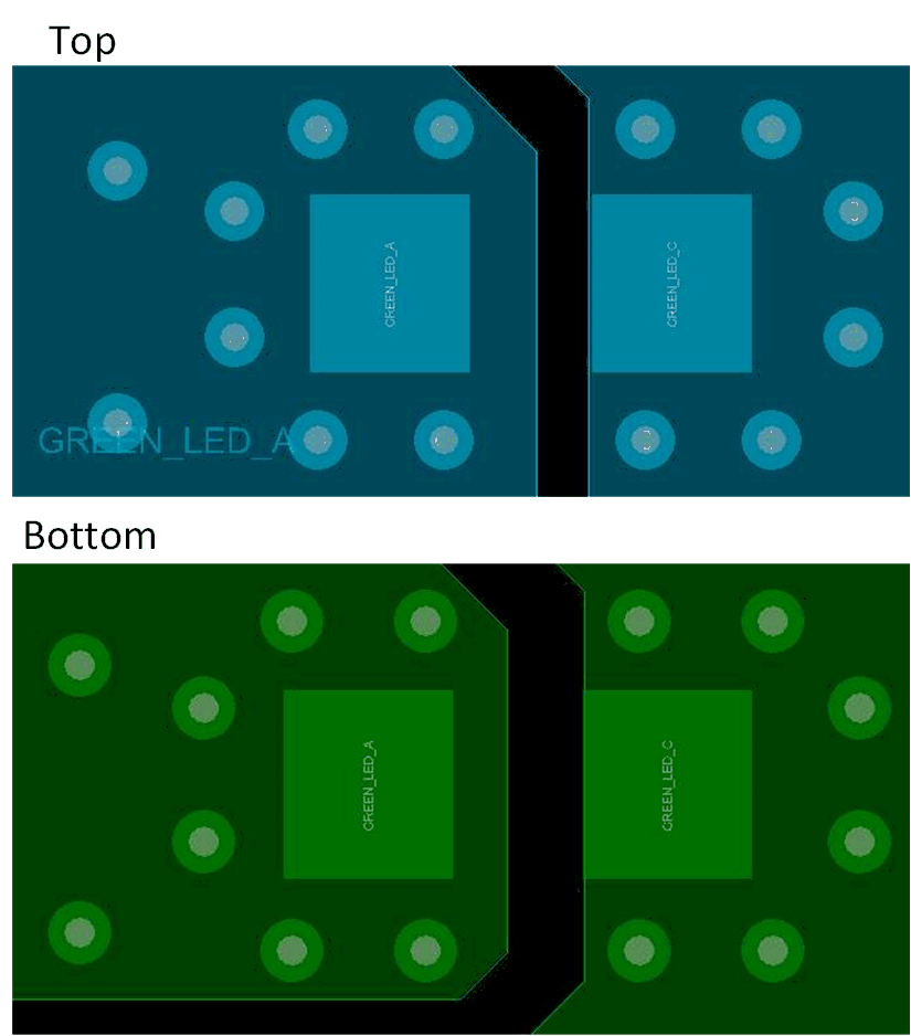
  • Place two identical capacitors directly opposite each other on the top and bottom side of the PCB. If there is only a single capacitor, it bends its middle towards the PCB and back. In doing this, the PCB is stimulated like the membrane of a loud speaker and emits acoustic waves. If two capacitors are placed opposite one another, both bend towards and away from the PCB at the same time. Thus, the PCB cannot resonate anymore.
  • The second action to reduce the residual noise further is to minimize the mechanical coupling of the ceramic capacitors and the PCB. By milling holes into the PCB besides the solder points, the stimulated PCB area is reduced significantly. Figure 4 shows the read marked holes in the PCB around the ceramic capacitors Top view.
Figure 9. LED Capacitor LayoutTIDA-080008 Cap_Layout.gif