ZHCSRR9J december 2003 – august 2023 TPS2061 , TPS2062 , TPS2063 , TPS2065 , TPS2066 , TPS2067
PRODMIX
- 1
- 1 特性
- 2 应用
- 3 说明
- 4 Revision History
- 5 说明(续)
- 6 Pin Configuration and Functions
- 7 Specifications
- 8 Parameter Measurement Information
- 9 Detailed Description
-
10Application and Implementation
- 10.1
Application Information
- 10.1.1 Power-supply Considerations
- 10.1.2 OC Response
- 10.1.3 Power Dissipation and Junction Temperature
- 10.1.4 Thermal Protection
- 10.1.5 Undervoltage Lockout (UVLO)
- 10.1.6 Universal Serial Bus (USB) Applications
- 10.1.7 Host/Self-Powered and Bus-powered Hubs
- 10.1.8 Low-power Bus-powered and High-Power Bus-Powered Functions
- 10.1.9 USB Power-distribution Requirements
- 10.1.10 Generic Hot-Plug Applications
- 10.1
Application Information
- 11Device and Documentation Support
- 12Mechanical, Packaging, and Orderable Information
7.5 Typical Characteristics(All Devices Excluding TPS2065DBV)
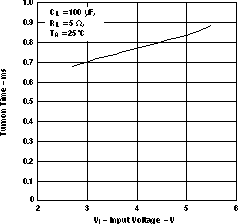 Figure 7-1 TURNON TIME vs INPUT
VOLTAGE
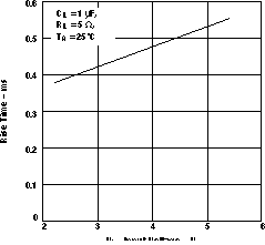 Figure 7-3 RISE TIME vs INPUT
VOLTAGE
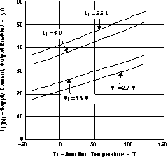 Figure 7-5 TPS2061, TPS2065 SUPPLY
CURRENT, OUTPUT ENABLED vs JUNCTION TEMPERATURE
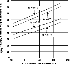 Figure 7-7 TPS2063, TPS2067 SUPPLY
CURRENT, OUTPUT ENABLED vs JUNCTION TEMPERATURE
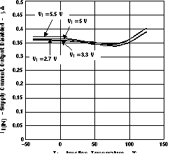 Figure 7-9 TPS2062, TPS2066 SUPPLY
CURRENT, OUTPUT DISABLED vs JUNCTION TEMPERATURE
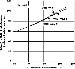 Figure 7-11 STATIC DRAIN-SOURCE
ON-STATE RESISTANCE vs JUNCTION TEMPERATURE
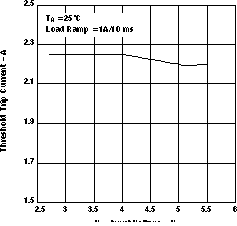 Figure 7-13 THRESHOLD TRIP CURRENT vs
INPUT VOLTAGE
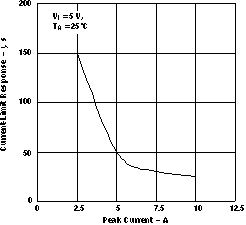 Figure 7-15 CURRENT-LIMIT RESPONSE vs
PEAK CURRENT
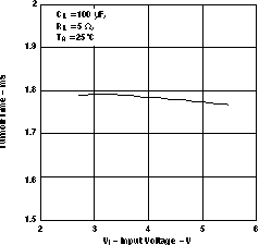 Figure 7-2 TURNOFF TIME vs INPUT
VOLTAGE
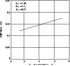 Figure 7-4 FALL TIME vs INPUT
VOLTAGE
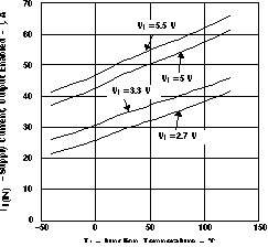 Figure 7-6 TPS2062, TPS2066 SUPPLY
CURRENT, OUTPUT ENABLED vs JUNCTION TEMPERATURE
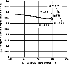 Figure 7-8 TPS2061, TPS2065 SUPPLY
CURRENT, OUTPUT DISABLED vs JUNCTION TEMPERATURE
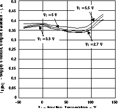 Figure 7-10 TPS2063, TPS2067 SUPPLY
CURRENT, OUTPUT DISABLED vs JUNCTION TEMPERATURE
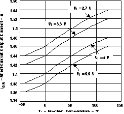 Figure 7-12 SHORT-CIRCUIT OUTPUT
CURRENT vsJUNCTION TEMPERATURE
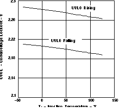 Figure 7-14 UNDERVOLTAGE LOCKOUT vs
JUNCTION TEMPERATURE
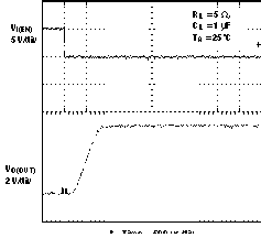 Figure 7-16 Turnon Delay and Rise Time With 1-μF Load
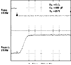 Figure 7-18 Turnon Delay and Rise Time With 100-μF Load
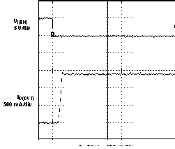 Figure 7-20 Short-Circuit Current, Device Enabled Into Short
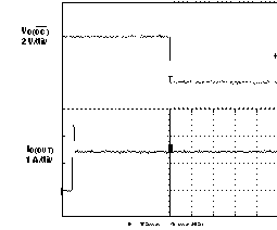 Figure 7-22 2-Ω
Load Connected to Enabled Device
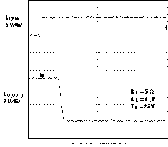 Figure 7-17 Turnoff Delay and Fall Time With 1-μF Load
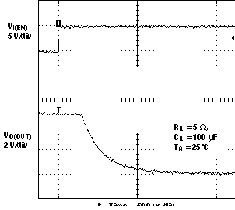 Figure 7-19 Turnoff Delay and Fall Time With 100-μF Load
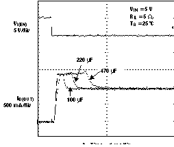 Figure 7-21 Inrush Current With Different Load Capacitance
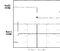 Figure 7-23 1-Ω
Load Connected to Enabled Device