ZHCSGI8A April 2017 – October 2021 ADC12D1620QML-SP
PRODUCTION DATA
- 1 特性
- 2 应用
- 3 说明
- 4 Revision History
- 5 Pin Configuration and Functions
-
6 Specifications
- 6.1 Absolute Maximum Ratings
- 6.2 ESD Ratings
- 6.3 Recommended Operating Conditions
- 6.4 Thermal Information
- 6.5 Converter Electrical Characteristics: Static Converter Characteristics
- 6.6 Converter Electrical Characteristics: Dynamic Converter Characteristics
- 6.7 Converter Electrical Characteristics: Analog Input/Output and Reference Characteristics
- 6.8 Converter Electrical Characteristic: Channel-to-Channel Characteristics
- 6.9 Converter Electrical Characteristics: LVDS CLK Input Characteristics
- 6.10 Electrical Characteristics: AutoSync Feature
- 6.11 Converter Electrical Characteristics: Digital Control and Output Pin Characteristics
- 6.12 Converter Electrical Characteristics: Power Supply Characteristics
- 6.13 Converter Electrical Characteristics: AC Electrical Characteristics
- 6.14 Electrical Characteristics: Delta Parameters
- 6.15 Timing Requirements: Serial Port Interface
- 6.16 Timing Requirements: Calibration
- 6.17 Quality Conformance Inspection
- 6.18 Timing Diagrams
- 6.19 Typical Characteristics
-
7 Detailed Description
- 7.1 Overview
- 7.2 Functional Block Diagram
- 7.3 Feature Description
- 7.4 Device Functional Modes
- 7.5
Programming
- 7.5.1
Control Modes
- 7.5.1.1
Non-ECM
- 7.5.1.1.1 Dual-Edge Sampling Pin (DES)
- 7.5.1.1.2 Non-Demultiplexed Mode Pin (NDM)
- 7.5.1.1.3 Dual Data-Rate Phase Pin (DDRPh)
- 7.5.1.1.4 Calibration Pin (CAL)
- 7.5.1.1.5 Low-Sampling Power-Saving Mode Pin (LSPSM)
- 7.5.1.1.6 Power-Down I-Channel Pin (PDI)
- 7.5.1.1.7 Power-Down Q-Channel Pin (PDQ)
- 7.5.1.1.8 Test-Pattern Mode Pin (TPM)
- 7.5.1.1.9 Full-Scale Input-Range Pin (FSR)
- 7.5.1.1.10 AC- or DC-Coupled Mode Pin (VCMO)
- 7.5.1.1.11 LVDS Output Common-Mode Pin (VBG)
- 7.5.1.2 Extended Control Mode
- 7.5.1.1
Non-ECM
- 7.5.1
Control Modes
- 7.6 Register Maps
- 8 Application Information Disclaimer
- 9 Power Supply Recommendations
- 10Layout
- 11Device and Documentation Support
- 12Mechanical, Packaging, and Orderable Information
6.6 Converter Electrical Characteristics: Dynamic Converter Characteristics
The following specifications apply after calibration for VA = VDR = VTC = VE = 1.9 V; I and Q channels AC-coupled, FSR pin = high; CL = 10 pF; differential AC-coupled sine wave input clock, fCLK = 1.6 GHz at 0.5 VP-P with 50% duty cycle; VBG = floating; non-extended control mode; Rext = Rtrim = 3300 Ω ±0.1%; analog signal source impedance = 100-Ω differential; 1:2 demultiplex non-DES mode; I and Q channels; duty-cycle stabilizer on.(1)(2)
| PARAMETER | TEST CONDITIONS | SUB-GROUPS | MIN | TYP(3) | MAX | UNIT | |||
|---|---|---|---|---|---|---|---|---|---|
| CER | Code error rate | 10–18 | Error/ Sample | ||||||
| IMD3 | 3rd order intermodulation distortion | fIN = 2070 MHz ± 2.5 MHz at –13 dBFS | –76 | dBFS | |||||
| –63 | dBc | ||||||||
| fIN = 2070 MHz ± 2.5 MHz at –16 dBFS | –80 | dBFS | |||||||
| –64 | dBc | ||||||||
| fIN = 2670 MHz ± 2.5 MHz at –13 dBFS | –72 | dBFS | |||||||
| –59 | dBc | ||||||||
| fIN = 2670 MHz ± 2.5 MHz at –16 dBFS | –77 | dBFS | |||||||
| –61 | dBc | ||||||||
| 1:2 DEMUX, NON-DES MODE, NON-ECM, NON-LSPSM, fCLK = 1.6 GHz, fIN = 248 MHz, VIN = –0.5 dBFS | |||||||||
| ENOB | Effective number of bits | [4] | 8.8 | 9.1 | bits | ||||
| [5] | 8.7 | ||||||||
| [6] | 8.4 | ||||||||
| SINAD | Signal-to-noise plus distortion ratio | [4] | 54.7 | 56.5 | dBFS | ||||
| [5] | 54.1 | ||||||||
| [6] | 52.3 | ||||||||
| SNR | Signal-to-noise ratio | [4] | 56 | 58.4 | dBFS | ||||
| [5] | 54.6 | ||||||||
| [6] | 53.5 | dBFS | |||||||
| THD | Total harmonic distortion | [4, 5] | –62 | –59.2 | dBFS | ||||
| [6] | –55.5 | dBFS | |||||||
| 2nd Harm | Second harmonic distortion | –72.2 | dBFS | ||||||
| 3rd Harm | Third harmonic distortion | –62.1 | dBFS | ||||||
| SFDR | Spurious-free dynamic range | [4] | 58.9 | 62.1 | dBFS | ||||
| [5] | 58.1 | ||||||||
| [6] | 56 | dBFS | |||||||
| 1:2 DEMUX, NON-DES MODE, NON-ECM, LSPSM, fCLK = 800 MHz, fIN = 248 MHz, VIN = –0.5 dBFS | |||||||||
| ENOB | Effective number of bits | [4, 5] | 9.1 | 9.5 | bits | ||||
| [6] | 8.6 | bits | |||||||
| SINAD | Signal-to-noise plus distortion ratio | [4, 5] | 56.5 | 58.6 | dBFS | ||||
| [6] | 53.5 | dBFS | |||||||
| SNR | Signal-to-noise ratio | [4, 5] | 57.6 | 59.8 | dBFS | ||||
| [6] | 56.8 | dBFS | |||||||
| THD | Total harmonic distortion | [4, 5] | –67 | –62.3 | dBFS | ||||
| [6] | –57 | dBFS | |||||||
| 2nd Harm | Second harmonic distortion | –77.7 | dBFS | ||||||
| 3rd Harm | Third harmonic distortion | –67.5 | dBFS | ||||||
| SFDR | Spurious-free dynamic range | [4, 5] | 62.5 | 67.4 | dBFS | ||||
| [6] | 57.5 | dBFS | |||||||
| NON-DEMUX, NON-DES MODE, ECM, NON-LSPSM, fCLK = 1.6 GHz, fIN = 248 MHz, VIN = –0.5 dBFS | |||||||||
| ENOB | Effective number of bits | 9.1 | bits | ||||||
| SINAD | Signal-to-noise plus distortion ratio | 56.6 | dBFS | ||||||
| SNR | Signal-to-noise ratio | 58.6 | dBFS | ||||||
| THD | Total harmonic distortion | –63.2 | dBFS | ||||||
| 2nd Harm | Second harmonic distortion | –72 | dBFS | ||||||
| 3rd Harm | Third harmonic distortion | –63.3 | dBFS | ||||||
| SFDR | Spurious-free dynamic range | 63.3 | dBFS | ||||||
| 1:4 DEMUX, DES MODE, NON-LSPSM, fCLK = 1.6 GHz, fIN = 248 MHz, VIN = –0.5 dBFS | |||||||||
| ENOB | Effective number of bits | 8.9 | bits | ||||||
| SINAD | Signal-to-noise plus distortion ratio | 55.5 | dB | ||||||
| SNR | Signal-to-noise ratio | 56.9 | dBFS | ||||||
| THD | Total harmonic distortion | –62.3 | dBFS | ||||||
| 2nd Harm | Second harmonic distortion | –79.1 | dBFS | ||||||
| 3rd Harm | Third harmonic distortion | –62.3 | dBFS | ||||||
| SFDR | Spurious-free dynamic range | 61.7 | dBFS | ||||||
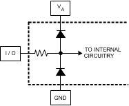
(1) The analog inputs are protected as shown below. Input voltage magnitudes beyond the
Absolute Maximum Ratings may damage this device.
(2) To ensure accuracy, it is required that VA, VTC, VE and VDR be well bypassed. Each supply pin must be decoupled with separate bypass capacitors.
(3) Typical figures are at TA = 25°C, and represent most likely parametric norms. Test limits are ensured to Texas Instrument's average outgoing quality level (AOQL).