ZHCSGI8A April   2017  – October 2021 ADC12D1620QML-SP

PRODUCTION DATA  

  1. 特性
  2. 应用
  3. 说明
  4. Revision History
  5. Pin Configuration and Functions
  6. Specifications
    1. 6.1  Absolute Maximum Ratings
    2. 6.2  ESD Ratings
    3. 6.3  Recommended Operating Conditions
    4. 6.4  Thermal Information
    5. 6.5  Converter Electrical Characteristics: Static Converter Characteristics
    6. 6.6  Converter Electrical Characteristics: Dynamic Converter Characteristics
    7. 6.7  Converter Electrical Characteristics: Analog Input/Output and Reference Characteristics
    8. 6.8  Converter Electrical Characteristic: Channel-to-Channel Characteristics
    9. 6.9  Converter Electrical Characteristics: LVDS CLK Input Characteristics
    10. 6.10 Electrical Characteristics: AutoSync Feature
    11. 6.11 Converter Electrical Characteristics: Digital Control and Output Pin Characteristics
    12. 6.12 Converter Electrical Characteristics: Power Supply Characteristics
    13. 6.13 Converter Electrical Characteristics: AC Electrical Characteristics
    14. 6.14 Electrical Characteristics: Delta Parameters
    15. 6.15 Timing Requirements: Serial Port Interface
    16. 6.16 Timing Requirements: Calibration
    17. 6.17 Quality Conformance Inspection
    18. 6.18 Timing Diagrams
    19. 6.19 Typical Characteristics
  7. Detailed Description
    1. 7.1 Overview
      1. 7.1.1 Operation Summary
    2. 7.2 Functional Block Diagram
    3. 7.3 Feature Description
      1. 7.3.1 Input Control and Adjust
        1. 7.3.1.1 AC- and DC-Coupled Modes
        2. 7.3.1.2 Input Full-Scale Range Adjust
        3. 7.3.1.3 Input Offset Adjust
        4. 7.3.1.4 Low-Sampling Power-Saving Mode (LSPSM)
        5. 7.3.1.5 DES Timing Adjust
        6. 7.3.1.6 Sampling Clock Phase Adjust
      2. 7.3.2 Output Control and Adjust
        1. 7.3.2.1 SDR / DDR Clock
        2. 7.3.2.2 LVDS Output Differential Voltage
        3. 7.3.2.3 LVDS Output Common-Mode Voltage
        4. 7.3.2.4 Output Formatting
        5. 7.3.2.5 Test-Pattern Mode
        6. 7.3.2.6 Time Stamp
      3. 7.3.3 Calibration Feature
        1. 7.3.3.1 Calibration Control Pins and Bits
        2. 7.3.3.2 How to Execute a Calibration
        3. 7.3.3.3 On-Command Calibration
        4. 7.3.3.4 Calibration Adjust
          1. 7.3.3.4.1 Read/Write Calibration Settings
        5. 7.3.3.5 Calibration and Power-Down
        6. 7.3.3.6 Calibration and the Digital Outputs
      4. 7.3.4 Power Down
      5. 7.3.5 Low-Sampling Power-Saving Mode (LSPSM)
    4. 7.4 Device Functional Modes
      1. 7.4.1 DES/Non-DES Mode
      2. 7.4.2 Demux/Non-Demux Mode
    5. 7.5 Programming
      1. 7.5.1 Control Modes
        1. 7.5.1.1 Non-ECM
          1. 7.5.1.1.1  Dual-Edge Sampling Pin (DES)
          2. 7.5.1.1.2  Non-Demultiplexed Mode Pin (NDM)
          3. 7.5.1.1.3  Dual Data-Rate Phase Pin (DDRPh)
          4. 7.5.1.1.4  Calibration Pin (CAL)
          5. 7.5.1.1.5  Low-Sampling Power-Saving Mode Pin (LSPSM)
          6. 7.5.1.1.6  Power-Down I-Channel Pin (PDI)
          7. 7.5.1.1.7  Power-Down Q-Channel Pin (PDQ)
          8. 7.5.1.1.8  Test-Pattern Mode Pin (TPM)
          9. 7.5.1.1.9  Full-Scale Input-Range Pin (FSR)
          10. 7.5.1.1.10 AC- or DC-Coupled Mode Pin (VCMO)
          11. 7.5.1.1.11 LVDS Output Common-Mode Pin (VBG)
        2. 7.5.1.2 Extended Control Mode
          1. 7.5.1.2.1 Serial Interface
    6. 7.6 Register Maps
      1. 7.6.1 Register Definitions
  8. Application Information Disclaimer
    1. 8.1 Application Information
      1. 8.1.1 Analog Inputs
        1. 8.1.1.1 Acquiring the Input
        2. 8.1.1.2 Driving the ADC in DES Mode
        3. 8.1.1.3 FSR and the Reference Voltage
        4. 8.1.1.4 Out-Of-Range Indication
        5. 8.1.1.5 AC-Coupled Input Signals
        6. 8.1.1.6 DC-Coupled Input Signals
        7. 8.1.1.7 Single-Ended Input Signals
      2. 8.1.2 Clock Inputs
        1. 8.1.2.1 CLK Coupling
        2. 8.1.2.2 CLK Frequency
        3. 8.1.2.3 CLK Level
        4. 8.1.2.4 CLK Duty Cycle
        5. 8.1.2.5 CLK Jitter
        6. 8.1.2.6 CLK Layout
      3. 8.1.3 LVDS Outputs
        1. 8.1.3.1 Common-Mode and Differential Voltage
        2. 8.1.3.2 Output Data Rate
        3. 8.1.3.3 Terminating Unused LVDS Output Pins
      4. 8.1.4 Synchronizing Multiple ADC12D1620 Devices in a System
        1. 8.1.4.1 AutoSync Feature
        2. 8.1.4.2 DCLK Reset Feature
      5. 8.1.5 Temperature Sensor
    2. 8.2 Radiation Environments
      1. 8.2.1 Total Ionizing Dose
      2. 8.2.2 Single Event Latch-Up and Functional Interrupt
      3. 8.2.3 Single Event Upset
    3. 8.3 Cold Sparing
  9. Power Supply Recommendations
    1. 9.1 System Power-On Considerations
      1. 9.1.1 Control Pins
      2. 9.1.2 Power On in Non-ECM
      3. 9.1.3 Power On in ECM
      4. 9.1.4 Power-on and Data Clock (DCLK)
  10. 10Layout
    1. 10.1 Layout Guidelines
      1. 10.1.1 Power Planes
      2. 10.1.2 Bypass Capacitors
      3. 10.1.3 Ground Planes
      4. 10.1.4 Power System Example
    2. 10.2 Layout Example
    3. 10.3 Thermal Considerations
    4. 10.4 Board Mounting Recommendation
  11. 11Device and Documentation Support
    1. 11.1 Device Support
      1. 11.1.1 Device Nomenclature
      2. 11.1.2 第三方产品免责声明
    2. 11.2 接收文档更新通知
    3. 11.3 支持资源
    4. 11.4 Trademarks
    5. 11.5 静电放电警告
    6. 11.6 术语表
  12. 12Mechanical, Packaging, and Orderable Information
    1. 12.1 Engineering Samples

Power-on and Data Clock (DCLK)

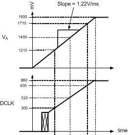
Many applications use the DCLK output for a system clock. For the ADC12D1620 device, each I channel and Q channel has its own DCLKI and DCLKQ, respectively. The DCLK output is always active, unless that channel is powered down or the DCLK reset feature is used while the device is in demux mode. As the supply to the device ramps, the DCLK also comes up. While the supply is too low, there is no output at DCLK. As the supply continues to ramp, DCLK functions intermittently with irregular frequency, but the amplitude continues to track with the supply. Much below the low end of operating supply range of the ADC12D1620, the DCLK is already fully operational.
GUID-02703F04-29F2-4B62-8C8A-8C47782FD6D3-low.gifFigure 9-1 Supply and DCLK Ramping