ZHCSGI8A April 2017 – October 2021 ADC12D1620QML-SP
PRODUCTION DATA
- 1 特性
- 2 应用
- 3 说明
- 4 Revision History
- 5 Pin Configuration and Functions
-
6 Specifications
- 6.1 Absolute Maximum Ratings
- 6.2 ESD Ratings
- 6.3 Recommended Operating Conditions
- 6.4 Thermal Information
- 6.5 Converter Electrical Characteristics: Static Converter Characteristics
- 6.6 Converter Electrical Characteristics: Dynamic Converter Characteristics
- 6.7 Converter Electrical Characteristics: Analog Input/Output and Reference Characteristics
- 6.8 Converter Electrical Characteristic: Channel-to-Channel Characteristics
- 6.9 Converter Electrical Characteristics: LVDS CLK Input Characteristics
- 6.10 Electrical Characteristics: AutoSync Feature
- 6.11 Converter Electrical Characteristics: Digital Control and Output Pin Characteristics
- 6.12 Converter Electrical Characteristics: Power Supply Characteristics
- 6.13 Converter Electrical Characteristics: AC Electrical Characteristics
- 6.14 Electrical Characteristics: Delta Parameters
- 6.15 Timing Requirements: Serial Port Interface
- 6.16 Timing Requirements: Calibration
- 6.17 Quality Conformance Inspection
- 6.18 Timing Diagrams
- 6.19 Typical Characteristics
-
7 Detailed Description
- 7.1 Overview
- 7.2 Functional Block Diagram
- 7.3 Feature Description
- 7.4 Device Functional Modes
- 7.5
Programming
- 7.5.1
Control Modes
- 7.5.1.1
Non-ECM
- 7.5.1.1.1 Dual-Edge Sampling Pin (DES)
- 7.5.1.1.2 Non-Demultiplexed Mode Pin (NDM)
- 7.5.1.1.3 Dual Data-Rate Phase Pin (DDRPh)
- 7.5.1.1.4 Calibration Pin (CAL)
- 7.5.1.1.5 Low-Sampling Power-Saving Mode Pin (LSPSM)
- 7.5.1.1.6 Power-Down I-Channel Pin (PDI)
- 7.5.1.1.7 Power-Down Q-Channel Pin (PDQ)
- 7.5.1.1.8 Test-Pattern Mode Pin (TPM)
- 7.5.1.1.9 Full-Scale Input-Range Pin (FSR)
- 7.5.1.1.10 AC- or DC-Coupled Mode Pin (VCMO)
- 7.5.1.1.11 LVDS Output Common-Mode Pin (VBG)
- 7.5.1.2 Extended Control Mode
- 7.5.1.1
Non-ECM
- 7.5.1
Control Modes
- 7.6 Register Maps
- 8 Application Information Disclaimer
- 9 Power Supply Recommendations
- 10Layout
- 11Device and Documentation Support
- 12Mechanical, Packaging, and Orderable Information
5 Pin Configuration and Functions
The center ground pins are for thermal dissipation and must be soldered to a ground plane to ensure rated performance. See Layout Guidlines for more information.

| PIN | TYPE | DESCRIPTION | EQUIVALENT CIRCUIT | |
|---|---|---|---|---|
| NAME | NO. | |||
| ANALOG FRONT-END AND CLOCK PINS | ||||
| CLK+ CLK– |
U2/V1 | I | Differential converter sampling clock. In the non-DES mode, the analog inputs are sampled on the positive transitions of this clock signal. In the DES mode, the selected input is sampled on both transitions of this clock. This clock must be AC-coupled. |
|
| DCLK_RST+ DCLK_RST– |
V2/W1 | I | Differential DCLK reset. A positive pulse on this input is used to reset the DCLKI and DCLKQ outputs of two or more ADC12D1620 devices in order to synchronize them with other ADC12D1620 devices in the system. DCLKI and DCLKQ are always in phase with each other, unless one channel is powered down, and do not require a pulse from DCLK_RST to become synchronized. The pulse applied here must meet timing relationships with respect to the CLK input. Although supported, this feature has been superseded by AutoSync. |
|
| RCLK+ RCLK– |
Y4/W5 | I | Reference clock input. When the AutoSync feature is active, and the ADC12D1620 is in secondary mode, the internal divided clocks are synchronized with respect to this input clock. The delay on this clock may be adjusted when synchronizing multiple ADCs. This feature is available in ECM with the DRC bits of the AutoSync Control Register (Addr: Eh, Bits: 15:7). |
|
| RCOut1+, RCOut1– RCOut2+, RCOut2– |
Y5/U6 V6/V7 |
O | Reference clock output 1 and 2. These signals, when enabled, provide a reference clock. The RCOut rates for all of the available modes can be found in Table 7-8; the rates displayed in the table are independent of whether the ADC is in primary or secondary mode. RCOut1 and RCOut2 are used to drive the RCLK of ADC12D1620 to enable automatic synchronization for multiple ADCs (AutoSync feature). The impedance of each trace from RCOut1 and RCOut2 to the RCLK of ADC12D1620 should be 100-Ω differential. Having two clock outputs allows the auto-synchronization to propagate as a binary tree. Use the DOC bit of the AutoSync Control Register (Addr: Eh; Bit: 1) to enable or disable this feature; default is disabled. |
|
| Rext+ Rext– |
C3/D3 | I/O | External reference resistor terminals. Connect a 3.3-kΩ, ±0.1% resistor between Rext+, Rext–. The Rext resistor is used as a reference to trim internal circuits that affect the linearity of the converter; the value and precision of this resistor must not be compromised. |
|
| Rtrim+ Rtrim– |
C1/D2 | I/O | Input termination trim resistor terminals. Connect a 3.3-kΩ, ±0.1%resistor between Rtrim+/ Rtrim–. The Rtrim resistor is used to establish the calibrated 100-Ω input impedance of Vinl, VinQ, and CLK. These impedances may be fine-tuned by varying the value of the resistor by a corresponding percentage; however, the tuning range and performance is not tested for such an alternative values. |
|
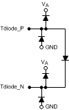
| Tdiode+ Tdiode– |
E2/F3 | O | Temperature sensor diode positive (anode) and negative (cathode) terminals. This set of pins is used for die temperature measurements. It has not been fully characterized. |
|
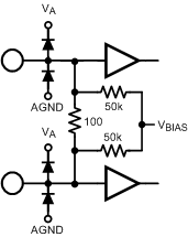
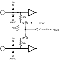
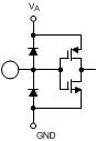
| VBG | B1 | I/O | Bandgap voltage output or LVDS common-mode voltage select. This pin provides a buffered version of the bandgap output voltage; it is capable of sourcing/sinking 100 μA and driving a load of up to 80 pF. Alternately, this pin may be used to select the LVDS digital output common-mode voltage. If tied to logic-high, the 1.2-V LVDS common-mode voltage is selected; 0.8 V is the default. |
|
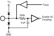
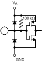
| VCMO | C2 | I/O | Common-mode voltage. This pin is the common-mode output in DC-coupling mode and also serves as the AC-coupling mode select pin. When DC-coupling is used at the analog inputs, the voltage output at this pin is required to be the common-mode input voltage at VIN+ and VIN−. When AC-coupling is used, this pin must be grounded. This pin is capable of sourcing or sinking 100 μA. |
|
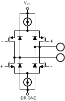
| VinI+, VinI– VinQ+, VinQ– |
H1/J1 N1/M1 |
I |
Differential signal I and Q inputs. In the non-dual edge sampling (non-DES) mode, each I and Q input is sampled and converted by its respective channel with each positive transition of the CLK input. In non-ECM (non-extended control mode) and DES mode, both channels sample the I input. In Extended Control mode (ECM), the Q input may optionally be selected for conversion in DES mode by the DEQ Bit of the Configuration Register (Addr: 0h; Bit: 6). Each I- and Q-channel input has an internal common mode bias that is disabled when DC-coupled mode is selected. Both inputs must be either AC- or DC-coupled. The coupling mode is selected by the VCMO pin. In non-ECM, the full-scale range of these inputs is determined by the FSR pin; both I and Q channels have the same full-scale input range. In ECM, the full-scale input range of the I- and Q-channel inputs may be independently set with the I- and Q-channel Full-Scale Range Adjust Registers (Addr: 3h and Addr: Bh, respectively). The high and low full-scale input range setting in non-ECM corresponds to the mid and minimum full-scale input range in ECM. The input offset may also be adjusted in ECM with the I- and Q-channel Offset Adjust Registers (Addr: 2h and Addr: Ah, respectively). |
|
| CONTROL AND STATUS PINS | ||||
| CAL | D6 | I | Calibration cycle initiate. The user can command the device to execute a self-calibration cycle by holding this input high for a minimum of tCAL_H after having held it low for a minimum of tCAL_L. This pin is active in both ECM and non-ECM. In ECM, this pin is logically OR'd with the CAL Bit of the Configuration Register (Addr: 0h, Bit 15). Therefore, both the pin and bit must be set low and then either can be set high to execute an on-command calibration. TI recommends holding the CAL pin high during normal usage to reduce the chance that an SEU causes a calibration cycle. |
|
| CalRun | B5 | O | Calibration running indication. This output is logic-high while the calibration sequence is executing; otherwise, this output is logic-low. |
|
| DDRPh | W4 | I | DDR phase select. In
DDR, when this input is logic-low, it selects the 0° data-to-DCLK
phase relationship. When this input is logic-high, it selects the
90° data-to-DCLK phase relationship; that is, the DCLK transition
indicates the middle of the valid data outputs. In SDR, when this input is logic-low, the output transitions on the rising edge of DCLK. When this input is logic-high, output transition is on the falling edge of DCLK. This pin only has an effect when the chip is in 1:2 demuxed mode; that is, the NDM pin is set to logic-low. In ECM, this input is ignored and the DDR phase is selected through the Control Register by the DPS bit (Addr: 0h, Bit 14); the default is 0° mode. |
|
| DES | V5 | I | Dual edge sampling
(DES) mode select. In the non-extended control mode (Non-ECM), when
this input is set to logic-high, the DES mode of operation is
selected; this means that the VinI input is sampled by both channels
in a time-interleaved manner and the VinQ input is ignored. When this input is set to logic-low, the device is in non-DES mode; that is, I and Q channels operate independently. In the extended control mode (ECM), this input is ignored and DES mode selection is controlled through the DES bit of the Configuration Register (Addr: 0h; Bit: 7); default is non-DES mode operation. |
|
| ECE | B3 | I | Extended control
enable. Extended feature control through the SPI interface is
enabled and the device is in ECM when this signal is asserted
(logic-low). Please reference Table 7-1
for information on the behavior of the control pins when the
extended feature control is enabled. When this signal is de-asserted (logic-high), the SPI interface is disabled, all SPI registers are reset to their default values, and all available settings are controlled with the control pins. |

|
| FSR | Y3 | I |
Full-scale input range select. In non-ECM, when this input is set to logic-low or logic-high, the full-scale differential input range for both I- and Q-channel inputs is set to the lower or higher FSR value, respectively. In the ECM, this input is ignored and the full-scale range of the I- and Q-channelinputs is independently determined by the setting of the I- and Q-channel Full-Scale Range Adjust Registers (Addr: 3h and Addr: Bh, respectively). Note that the high (lower) FSR value in non-ECM corresponds to the mid (min) available selection in ECM; the FSR range in ECM is greater. |
|
| LSPSM | V4 | I | Low-sampling power-saving mode (LSPSM) select. In LSPSM, the power consumption is reduced by approximately 20%, and some improvement in performance may be seen. The output is in SDR in 1:2 demux mode and DDR in 1:1 non-demux mode. DDR is not available in 1:2 demux mode in LSPSM. The maximum sampling rate in LSPSM in non-DES mode is 800 MSPS. When this input is logic-high, the device is in LSPSM and when this input is logic-low, the device is in normal mode or non-LSPSM. |
|
| NDM | A5 | I | Non-demuxed mode select. Setting this input to logic-high causes the digital output bus to be in the 1:1 non-demuxed mode. Setting this input to logic-low causes the digital output bus to be in the 1:2 demuxed mode. This feature is pin-controlled only and remains active during both ECM and non-ECM. |
|
| PDI PDQ |
U3 V3 |
I | Power down I and Q channels. Setting either input to logic-high powers down the respective I or Q channel. Setting either input to logic-low brings the respective I or Q channel to a operational state after a finite time delay. This pin is active in both ECM and non-ECM. In ECM, each pin is logically OR'd with its respective bit. Therefore, either this pin or the PDI and PDQ bits in the Configuration Register (Addr: 0h; Bit: 11 and Bit: 10, respectively) can be used to power down the I and Q channels. |
|
| RSV | W3 | — | Reserved. This pin is used for internal purposes and must be connected to GND through a 100-kΩ resistor. | NONE |
| RSV1 | E3 | — | Decouple this pin with a 100-nF capacitor with a low resistance, low inductance path to GND. | NONE |
| RSV2 | F4 | — | Decouple this pin with a 100-nF capacitor with a low resistance, low inductance path to GND. | NONE |
| SCLK | C5 | I | Serial clock. In ECM, serial data is shifted into and out of the device synchronously to this clock signal. This clock may be disabled and held logic-low, as long as timing specifications are not violated when the clock is enabled or disabled. |
|
| SCS | C4 | I | Serial chip select. In ECM, when this signal is asserted (logic-low), SCLK is used to clock in serial data that is present on SDI and to source serial data on SDO. When this signal is de-asserted (logic-high), SDI is ignored and SDO is tri-state. |
|
| SDI | B4 | I | Serial data-in. In ECM, serial data is shifted into the device on this pin while SCS signal is asserted (logic-low). |
|
| SDO | A3 | O | Serial data-out. In ECM, serial data is shifted out of the device on this pin while SCS signal is asserted (logic-low). This output is tri-state when SCS is de-asserted (logic-high). |
|
| TPM | A4 | I | Test pattern mode select. With this input at logic-high, the device continuously outputs a fixed, repetitive test pattern at the digital outputs. In ECM, this input is ignored, and the test pattern mode can only be activated through the Control Register by the TPM bit (Addr: 0h, Bit: 12). |
|
| POWER AND GROUND PINS | ||||
| GND | A1, A7, B2, B7, C6, D4, D5, E4, K1, L1, T4, U4, U5, W2, W7, Y1, Y7, AA2:AL11 | P | Analog ground return | NONE |
| GNDDR | A13, A17, A20, D13, D16, E17, F17, F20, M17, M20, U13, U17, V18, Y13, Y17, Y20 | P | Ground return for the output drivers | NONE |
| GNDE | A9, B8, C9, V9, W8, Y9 | P | Ground return for the digital encoder | NONE |
| GNDTC | F2, G2, H3, J2, K4, L4, M2, N3, P2, R2, T2, T3, U1 | P | Ground return for the track-and-hold and clock circuitry | NONE |
| VA | A2, A6, B6, C7, D1, D8, D9, E1, F1, H4, N4, R1, T1, U8, U9, W6, Y2, Y6 | P | Analog power supply. This supply is tied to the ESD ring; therefore, it must be powered up before or with any other supply. | NONE |
| VbiasI | D7, J4, K2 | P | Bias voltage I channel. This is an externally decoupled bias voltage for the I channel. Each pin must individually be decoupled with a 100-nF capacitor through a low resistance, low inductance path to GND. | NONE |
| VbiasQ | L2, M4, U7 | P | Bias voltage Q channel. This is an externally decoupled bias voltage for the Q channel. Each pin must individually be decoupled with a 100-nF capacitor through a low resistance, low inductance path to GND. | NONE |
| VDR | A11, A15, C18, D11, D15, D17, J17, J20, R17, R20, T17, U11, U15, U16, Y11, Y15 | P | Power supply for the output drivers | NONE |
| VE | A8, B9, C8, V8, W9, Y8 | P | Power supply for the digital encoder | NONE |
| VTC | G1, G3, G4, H2, J3, K3, L3, M3, N2, P1, P3, P4, R3, R4 | P | Power supply for the track-and-hold and clock circuitry | NONE |
| HIGH-SPEED DIGITAL OUTPUT PINS | ||||
| DCLKI+, DCLKI– DCLKQ+, DCLKQ– |
K19/K20 L19/L20 |
O | Data clock output for the I- and Q-channel data bus. These differential clock outputs are used to latch the output data and, if used, terminate with a 100-Ω differential resistor placed as closely as possible to the differential receiver. Delayed and non-delayed data outputs are supplied synchronously to this signal. The DCLK rates for all of the available modes can be found in Table 7-8. DCLKI and DCLKQ are always in phase with each other, unless one channel is powered down, and do not require a pulse from DCLK_RST to become synchronized. |
|
| DI11+, DI11– DI10+, DI10– DI9+, DI9– DI8+, DI8– DI7+, DI7– DI6+, DI6– DI5+, DI5– DI4+, DI4– DI3+, DI3– DI2+, DI2– DI1+,DI1 – DI0+, DI0– · DQ11+, DQ11– DQ10+, DQ10– DQ9+, DQ9– DQ8+, DQ8– DQ7+, DQ7– DQ6+, DQ6– DQ5+, DQ5– DQ4+, DQ4– DQ3+, DQ3– DQ2+, DQ2– DQ1+, DQ1– DQ0+, DQ0– |
J18/J19 H19/H20 H17/H18 G19/G20 G17/G18 F18/F19 E19/E20 D19/D20 D18/E18 C19/C20 B19/B20 B18/C17 · M18/M19 N19/N20 N17/N18 P19/P20 P17/P18 R18/R19 T19/T20 U19/U20 U18/T18 V19/V20 W19/W20 W18/V17 |
O | I- and Q-channel digital data outputs. In non-demux mode, this LVDS data is transmitted at the sampling clock rate. In demux mode, these outputs provide ½ the data at ½ the sampling clock rate, synchronized with the delayed data; that is, the other ½ of the data which was sampled one clock cycle earlier. Compared with the DId and DQd outputs, these outputs represent the later time samples. If used, terminate each of these outputs with a 100-Ω differential resistor placed as closely as possible to the differential receiver. |
|
| DId11+, DId11– DId10+, DId10– DId9+, DId9– DId8+, DId8– DId7+, DId7– DId6+, DId6– DId5+, DId5– DId4+, DId4– DId3+, DId3– DId2+, DId2– DId1+,DId1 – DId0+, DId0– · DQd11+, DQd11– DQd10+, DQd10– DQd9+, DQd9– DQd8+, DQd8– DQd7+, DQd7– DQd6+, DQd6– DQd5+, DQd5– DQd4+, DQd4– DQd3+, DQd3– DQd2+, DQd2– DQd1+, DQd1– DQd0+, DQd0– |
A18/A19 B17/C16 A16/B16 B15/C15 C14/D14 A14/B14 B13/C13 C12/D12 A12/B12 B11/C11 C10/D10 A10/B10 · Y18/Y19 W17/V16 Y16/W16 W15/V15 V14/U14 Y14/W14 W13/V13 V12/U12 Y12/W12 W11/V11 V10/U10 Y10/W10 |
O | Delayed I- and Q-channel digital data outputs. In non-demux mode, these outputs are tri-state. In demux mode, these outputs provide ½ the data at ½ the sampling clock rate, synchronized with the non-delayed data; that is, the other ½ of the data which was sampled one clock cycle later. Compared with the DI and DQ outputs, these outputs represent the earlier time samples. If used, terminate each of these outputs with a 100-Ω differential resistor placed as closely as possible to the differential receiver. |
|
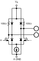
| ORI+, ORI– ORQ+, ORQ– |
K17/K18 L17/L18 |
O | Out-of-range output for the I and Q channel. This differential output is asserted logic-high while the over- or under-range condition exists; that is, the differential signal at each respective analog input exceeds the full-scale value. Each OR result refers to the current data, with which it is clocked out. If used, terminate each of these outputs with a 100-Ω differential resistor placed as closely as possible to the differential receiver. |
|