ZHCSFA6B June   2016  – July 2018 CC1350

PRODUCTION DATA.  

  1. 1器件概述
    1. 1.1 特性
    2. 1.2 应用
    3. 1.3 说明
    4. 1.4 功能框图
  2. 2修订历史记录
  3. 3Device Comparison
    1. 3.1 Related Products
  4. 4Terminal Configuration and Functions
    1. 4.1 Pin Diagram – RSM Package
    2. 4.2 Signal Descriptions – RSM Package
    3. 4.3 Pin Diagram – RHB Package
    4. 4.4 Signal Descriptions – RHB Package
    5. 4.5 Pin Diagram – RGZ Package
    6. 4.6 Signal Descriptions – RGZ Package
  5. 5Specifications
    1. 5.1  Absolute Maximum Ratings
    2. 5.2  ESD Ratings
    3. 5.3  Recommended Operating Conditions
    4. 5.4  Power Consumption Summary
    5. 5.5  RF Characteristics
    6. 5.6  Receive (RX) Parameters, 861 MHz to 1054 MHz
    7. 5.7  Receive (RX) Parameters, 431 MHz to 527 MHz
    8. 5.8  Transmit (TX) Parameters, 861 MHz to 1054 MHz
    9. 5.9  Transmit (TX) Parameters, 431 MHz to 527 MHz
    10. 5.10 1-Mbps GFSK (Bluetooth low energy) – RX
    11. 5.11 1-Mbps GFSK (Bluetooth low energy) – TX
    12. 5.12 PLL Parameters
    13. 5.13 ADC Characteristics
    14. 5.14 Temperature Sensor
    15. 5.15 Battery Monitor
    16. 5.16 Continuous Time Comparator
    17. 5.17 Low-Power Clocked Comparator
    18. 5.18 Programmable Current Source
    19. 5.19 DC Characteristics
    20. 5.20 Thermal Characteristics
    21. 5.21 Timing and Switching Characteristics
      1. 5.21.1 Reset Timing
        1. Table 5-1 Reset Timing
      2. 5.21.2 Wakeup Timing
        1. Table 5-2 Wakeup Timing
      3. 5.21.3 Clock Specifications
        1. Table 5-3 24-MHz Crystal Oscillator (XOSC_HF)
        2. Table 5-4 32.768-kHz Crystal Oscillator (XOSC_LF)
        3. Table 5-5 48-MHz RC Oscillator (RCOSC_HF)
        4. Table 5-6 32-kHz RC Oscillator (RCOSC_LF)
      4. 5.21.4 Flash Memory Characteristics
        1. Table 5-7 Flash Memory Characteristics
      5. 5.21.5 Synchronous Serial Interface (SSI) Characteristics
        1. Table 5-8 Synchronous Serial Interface (SSI) Characteristics
    22. 5.22 Typical Characteristics
    23. 5.23 Typical Characteristics – Sub-1 GHz
    24. 5.24 Typical Characteristics – 2.4 GHz
  6. 6Detailed Description
    1. 6.1  Overview
    2. 6.2  Main CPU
    3. 6.3  RF Core
    4. 6.4  Sensor Controller
    5. 6.5  Memory
    6. 6.6  Debug
    7. 6.7  Power Management
    8. 6.8  Clock Systems
    9. 6.9  General Peripherals and Modules
    10. 6.10 Voltage Supply Domains
    11. 6.11 System Architecture
  7. 7Application, Implementation, and Layout
    1. 7.1 Application Information
    2. 7.2 TI Design or Reference Design
  8. 8器件和文档支持
    1. 8.1  器件命名规则
    2. 8.2  工具和软件
    3. 8.3  文档支持
    4. 8.4  德州仪器 (TI) 低功耗射频网站
    5. 8.5  其他信息
    6. 8.6  社区资源
    7. 8.7  商标
    8. 8.8  静电放电警告
    9. 8.9  出口管制提示
    10. 8.10 术语表
  9. 9机械、封装和可订购信息
    1. 9.1 封装信息

Typical Characteristics – Sub-1 GHz

Unless otherwise stated, all performance figures represent an average over six typical parts at room temperature and with the internal DC/DC converter enabled.
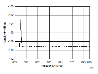
CC1350 D001_RX_sens_freq_863_876_SWRS183.gif
Figure 5-11 RX (50 kbps) Sensitivity
vs Frequency 863 MHz to 876 MHz
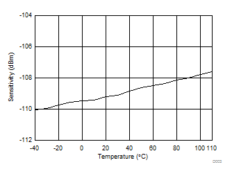
CC1350 D003_RX_sens_temp_868_SWRS183.gif
Figure 5-13 RX (50 kbps) Sensitivity vs Temperature 868 MHz
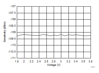
CC1350 D005_RX_sens_volt_868_SWRS183.gif
Figure 5-15 RX (50 kbps) Sensitivity vs Voltage 868 MHz
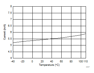
CC1350 D007_RX_curr_temp_868_SWRS183.gif
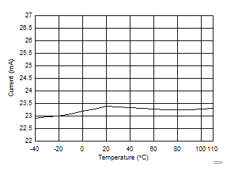
Figure 5-17 RX (50 kbps) Current vs Temperature at 868 MHz
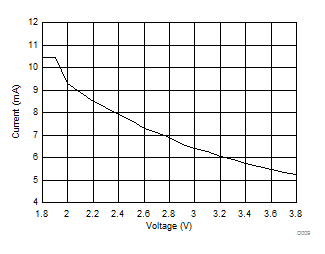
CC1350 D009_RX_curr_volt_868_SWRS183.gif
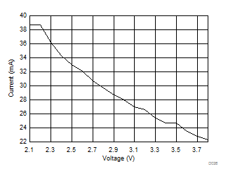
Figure 5-19 RX (50 kbps) Current vs Voltage at 868 MHz
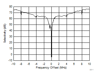
CC1350 D011_RX_sel_3dB_868_SWRS183.gif
Figure 5-21 RX (50 kbps) Selectivity With Wanted Signal at
868 MHz, 3 dB Above Sensitivity Limit
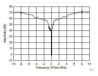
CC1350 D013_RX_sel_868_-96dBm_SWRS183.gif
Figure 5-23 RX (50 kbps) Selectivity With Wanted Signal at
868 MHz, –96 dBm
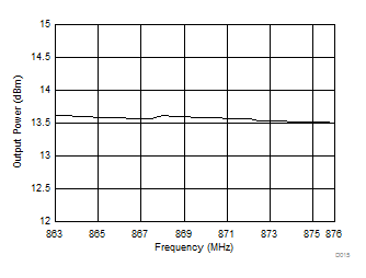
CC1350 D015_TX_max_out_863-876_SWRS183.gif
Figure 5-25 TX Maximum Output Power, 863 MHz to 876 MHz
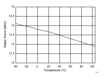
CC1350 D017_TX_max_out_868_SWRS183.gif
Figure 5-27 TX Maximum Output Power vs Temperature,
868 MHz
CC1350 D019_TX_out_VDDS_868_SWRS183.gif
Figure 5-29 TX Maximum Output Power vs VDDS, 868 MHz
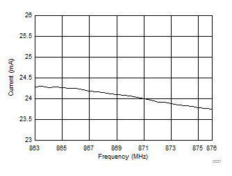
CC1350 D021_TX_curr_out_863-876_WRS183.gif
Figure 5-31 TX Current With Maximum Output Power,
863 MHz to 876 MHz
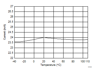
CC1350 D023_TX_curr_temp_868_wrs183.gif
Figure 5-33 TX Current With Maximum Output Power
vs Temperature, 868 MHz
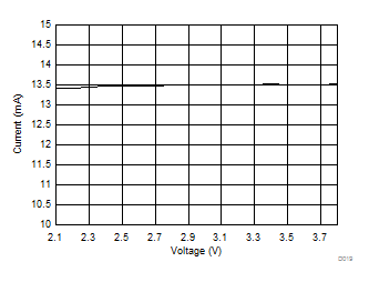
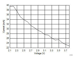
CC1350 D025_TX_curr_volt_868_wrs183.gif
Figure 5-35 TX Current With Maximum Output Power
vs Voltage, 868 MHz
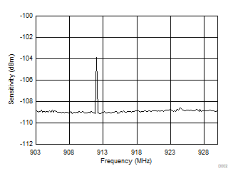
CC1350 D002_RX_sens_freq_902_928_SWRS183.gif
Figure 5-12 RX (50 kbps) Sensitivity
vs Frequency 902 MHz to 928 MHz
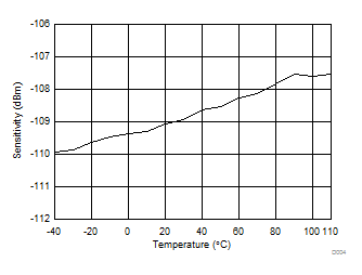
CC1350 D004_RX_sens_temp_915_SWRS183.gif
Figure 5-14 RX (50 kbps) Sensitivity vs Temperature 915 MHz
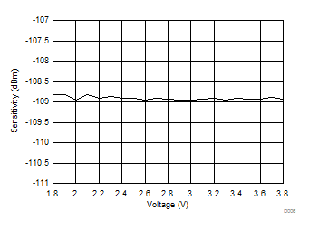
CC1350 D006_RX_sens_volt_915_SWRS183.gif
Figure 5-16 RX (50 kbps) Sensitivity vs Voltage 915 MHz
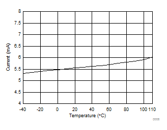
CC1350 D008_RX_curr_temp_915_SWRS183.gif
Figure 5-18 RX (50 kbps) Current vs Temperature at 915 MHz
CC1350 D010_RX_curr_volt_915_SWRS183.gif
Figure 5-20 RX (50 kbps) Current vs Voltage at 915 MHz
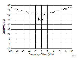
CC1350 D012_RX_sel_3dB_915_SWRS183.gif
Figure 5-22 RX (50 kbps) Selectivity With Wanted Signal at
915 MHz, 3 dB Above Sensitivity Limit
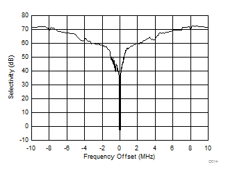
CC1350 D014_RX_sel_915_-96dBm_SWRS183.gif
Figure 5-24 RX (50 kbps) Selectivity With Wanted Signal at
915 MHz, –96 dBm
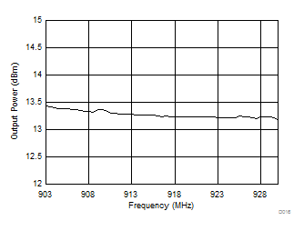
CC1350 D016_TX_max_out_902-928_SWRS183.gif
Figure 5-26 TX Maximum Output Power, 902 MHz to 928 MHz
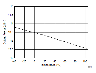
CC1350 D018_TX_max_out_915_SWRS183.gif
Figure 5-28 TX Maximum Output Power vs Temperature,
915 MHz
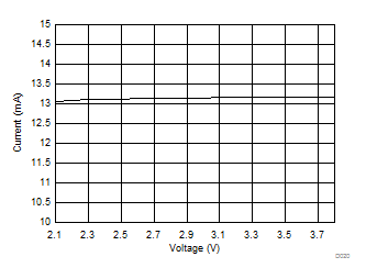
CC1350 D020_TX_out_VDDS_915_SWRS183.gif
Figure 5-30 TX Maximum Output Power vs VDDS, 915 MHz
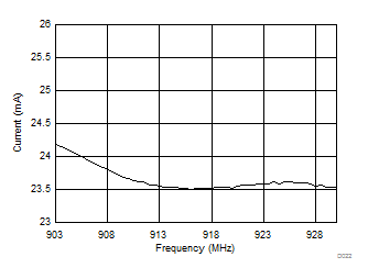
CC1350 D022_TX_curr_out_902-928_wrs183.gif
Figure 5-32 TX Current With Maximum Output Power,
902 MHz to 928 MHz
CC1350 D024_TX_curr_temp_915_wrs183.gif
Figure 5-34 TX Current With Maximum Output Power
vs Temperature, 915 MHz
CC1350 D026_TX_curr_volt_915_WRS183.gif
Figure 5-36 TX Current With Maximum Output Power
vs Voltage, 915 MHz

SPACER