TIDUEM8B March 2019 – February 2021
2.3.1.4.2 Current Measurement Analog Front End
The analog front end for current inputs is different from the analog front end for the voltage inputs. Figure 2-6 shows the analog front end used for a current channel, where the positive and negative leads from a CT are connected to pins 1 and 3 of header J26.
 Figure 2-6 Analog Front End for Current Inputs
The analog front end for current consists of footprints for electromagnetic interference filter beads (R89 and R90), burden resistors for current transformers (R91 and R92), and an RC low-pass filter (R94, R95, C97, C98, and C99) that functions as an anti-alias filter. There are also footprints (U21 and U22) that can be replaced with the TVS0500 for supplemental protection from surges, if required.
As Figure 2-6 shows, resistors R91 and R92 are the burden resistors, which are in series with each other. For best THD performance, instead of using one burden resistor, two identical burden resistors in series are used with the common point being connected to GND. This split-burden resistor configuration ensures that the waveforms fed to the positive and negative terminals of the ADC are 180 degrees out of phase with each other, which would provide the best THD results with this ADC. The total burden resistance is selected based on the current range used and the turns ratio specification of the CT (this design uses CTs with a turns ratio of 2000). The total value of the burden resistor for this design is 12.98 Ω.
Equation 2 shows how to calculate the range of differential voltages fed to the current ADC channel for a given maximum current, CT turns ratio, and burden resistor value.
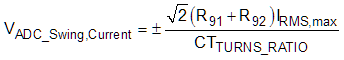
Based on the maximum current of 100 A, CT turns ratio of 2000, and burden resistor of 12.98 Ω, of this design, the input signal to the current ADC has a voltage swing of ±918 mV maximum (649 mVRMS) when the maximum current rating of the meter (100 A) is applied. This ±918-mV maximum input voltage is well within the ±1.2-V input range of the device for the selected PGA gain of 1 that is used for the current channels.
Note that the pin order of the AINxP and AINxN pins on the ADS131M04 is swapped when going from one converter to another. As an example, AIN0P is pin 3 and AIN0N is pin 4 but AIN1N is pin 5 and AIN1P is pin 6. The swapped order is why the order of the CT positive output terminal and negative output terminal is swapped between the J26 current input terminal block of Phase A and the J27 current input terminal block of Phase B.