TIDT193 August 2020 – MONTH
3.2 Switch Node
The following image shows the FET switch node voltage (YELLOW) at TP3 and the input voltage (BLUE). The input voltage is 18 V and the 14-V output is loaded to 130 mA.
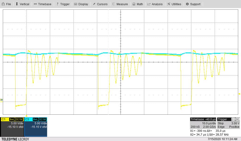 Figure 3-7 FET Switch Node Voltage (Vsnode: 5 V/div, VIN: 5 V/div, 10 μs/div)
The following image (scope persistence on) shows the FET switch node voltage (YELLOW) at TP3 and the input voltage (BLUE). The input voltage is 18 V and the 14-V output is loaded to 130 mA. This shows the effects of valley switching and frequency dithering on the switch node waveform.
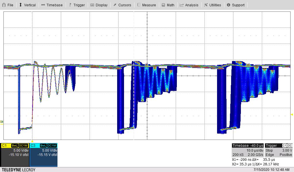 Figure 3-8 FET Switch Node Voltage (Vsnode: 5 V/div, VIN: 5 V/div, 10 μs/div)
 The following image shows the FET switch node voltage (YELLOW) at TP3 and the input voltage (BLUE). The input voltage is 18 V and the 14-V output is loaded to 0 mA.
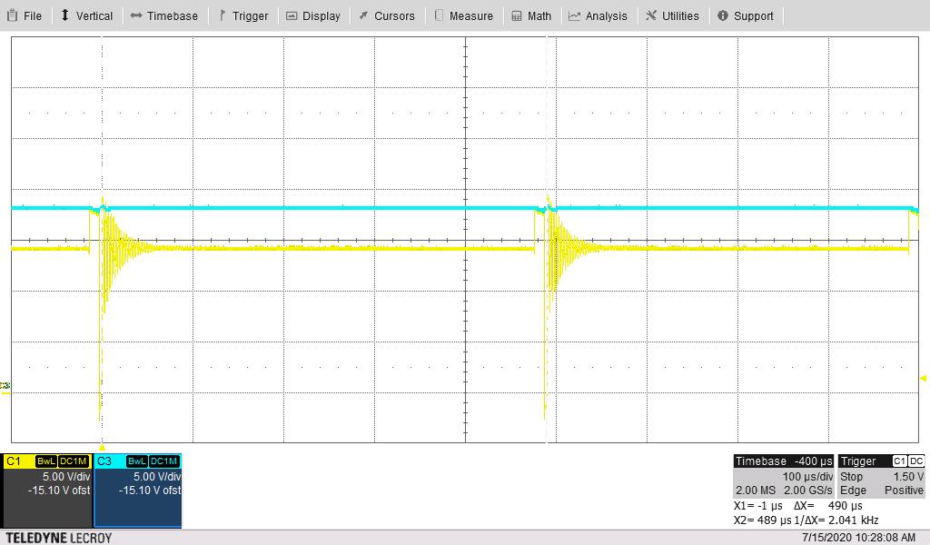 Figure 3-9 FET Switch Node Voltage (Vsnode: 5 V/div, VIN: 5 V/div, 100 μs/div) .
 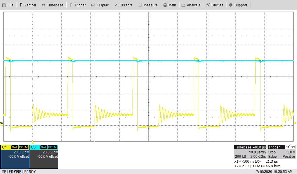 Figure 3-10 FET Switch Node Voltage (Vsnode: 20 V/div, VIN: 20 V/div, 10 μs/div) .
 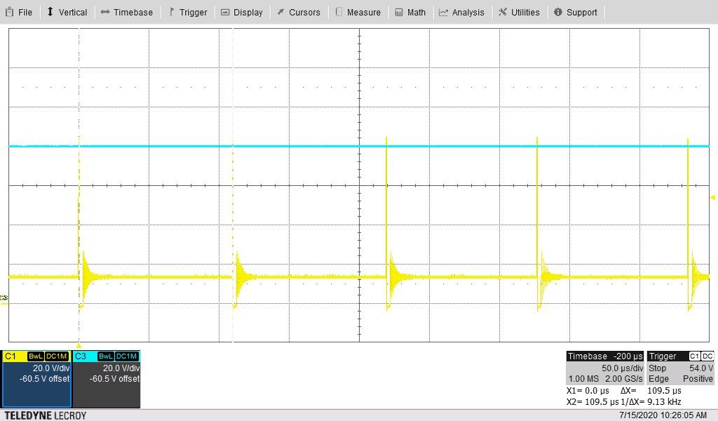 Figure 3-11 FET Switch Node Voltage (Vsnode: 20 V/div, VIN: 20 V/div, 50 μs/div) .
 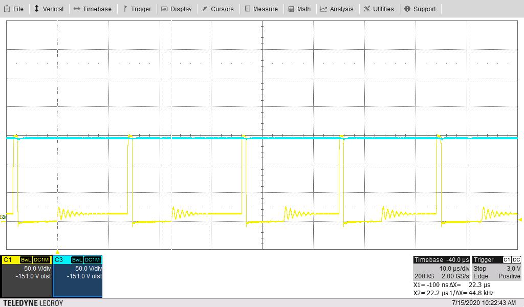 Figure 3-12 FET Switch Node Voltage (Vsnode: 50 V/div, VIN: 50 V/div, 10 μs/div) .
 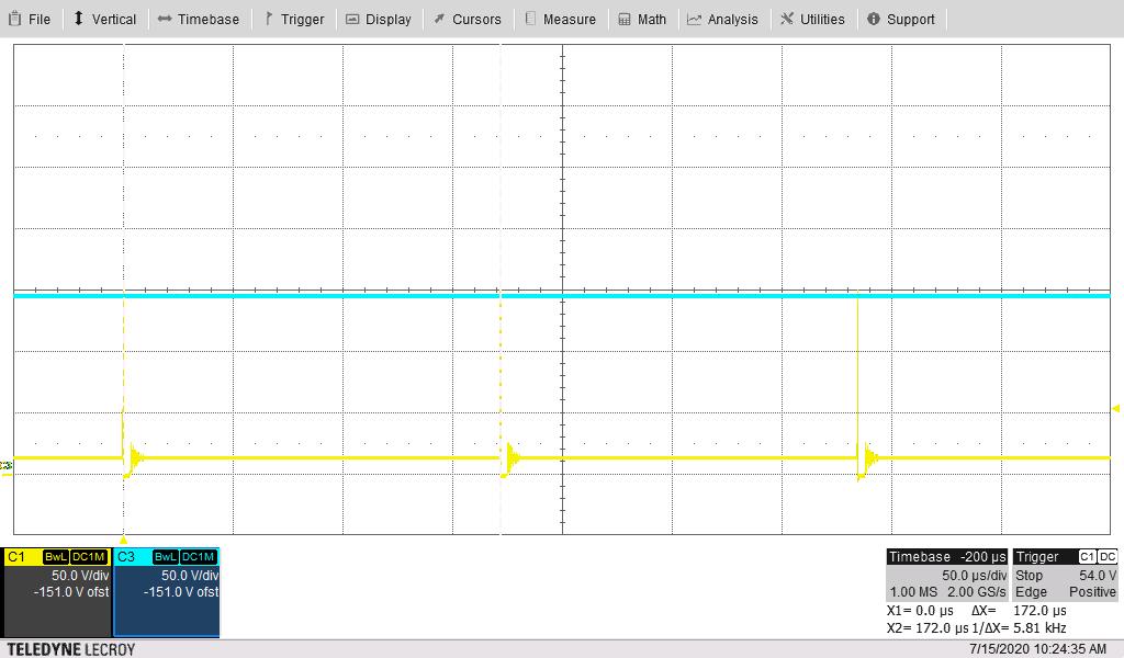 Figure 3-13 FET Switch Node Voltage (Vsnode: 50 V/div, VIN: 50 V/div, 50 μs/div) .
 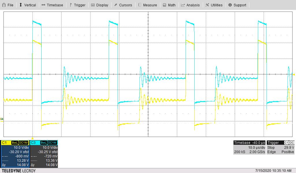 Figure 3-14 Switching Voltages (Vsnode: 10 V/div, D1-Cathode: 10 V/div, 10 μs/div) .
 The following image shows shows the switching voltages on each side of resistor divider R1/R2. The waveforms show the switch node voltage at TP3 (YELLOW) and the voltage at R1 (side connected to D2) (BLUE). The input voltage is 50 V and the 14-V output is loaded to 130 mA.
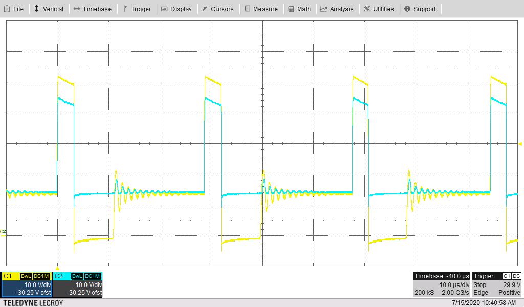 Figure 3-15 Switching Voltages (Vsnode: 10 V/div, D1-Cathode: 10 V/div, 10 μs/div) .