SPRUJF1C November   2024  – December 2025 AM2612


  1.   1
  2.   Description
  3.   Get Started
  4.   Features
  5.   5
  6. 1Evaluation Module Overview
    1. 1.1 Introduction
      1. 1.1.1 Preface: Read This First
        1. 1.1.1.1 Sitara MCU+ Academy
        2. 1.1.1.2 Important Usage Notes
    2. 1.2 Kit Contents
    3. 1.3 Device Information
      1. 1.3.1 System Architecture Overview
      2. 1.3.2 Component Identification
      3. 1.3.3 Functional Block Diagram
      4. 1.3.4 BoosterPacks
      5. 1.3.5 Device Information
        1. 1.3.5.1 Security
  7. 2Hardware
    1. 2.1  Setup
      1. 2.1.1 Standalone Configuration
    2. 2.2  Power Requirements
      1. 2.2.1 Power Input Using USB Type-C Connector
      2. 2.2.2 Power Tree
      3. 2.2.3 Power Status LEDs
    3. 2.3  Header Information
      1. 2.3.1 OSPI Expansion Connector
      2. 2.3.2 ADC/DAC External VREF Headers
      3. 2.3.3 FSI Header
      4. 2.3.4 EQEP Headers
    4. 2.4  Push Buttons
    5. 2.5  Reset
    6. 2.6  Clock
    7. 2.7  Boot Mode Selection
    8. 2.8  GPIO Mapping
    9. 2.9  IO Expander
    10. 2.10 Interfaces
      1. 2.10.1  Memory Interfaces
        1. 2.10.1.1 OSPI
        2. 2.10.1.2 Board ID EEPROM
      2. 2.10.2  Ethernet Interface
        1. 2.10.2.1 Ethernet PHY 0 - RGMII2 / PR0_PRU0
        2. 2.10.2.2 Ethernet PHY 1 - RGMII1 / PR0_PRU1
      3. 2.10.3  I2C
        1. 2.10.3.1 Industrial Application LEDs
      4. 2.10.4  SPI
      5. 2.10.5  UART
      6. 2.10.6  MCAN
      7. 2.10.7  SDFM
      8. 2.10.8  FSI
      9. 2.10.9  JTAG
      10. 2.10.10 Test Automation Pin Mapping
      11. 2.10.11 LIN
      12. 2.10.12 ADC and DAC
      13. 2.10.13 EQEP
      14. 2.10.14 EPWM
      15. 2.10.15 USB
    11. 2.11 BoosterPack Headers
      1. 2.11.1 BoosterPack Mode 00: Standard LaunchPad/BoosterPack Pinout
      2. 2.11.2 BoosterPack Mode 01: Servo Motor Control BoosterPacks Mode
      3. 2.11.3 BoosterPack Mode 10: BOOSTXL-IOLINKM-8 Mode
      4. 2.11.4 BoosterPack Mode 11: C2000 DRVx BoosterPacks Mode
    12. 2.12 Pinmux Mapping
    13. 2.13 Test Points
    14. 2.14 Best Practices
  8. 3Software
  9. 4Hardware Design Files
  10. 5Compliance
  11. 6Additional Information
    1. 6.1 Revision E1 Appendix
      1. 6.1.1 TA_POWERDOWNz pulled up by VSYS_TA_3V3 which is powered by VSYS_3V3
      2. 6.1.2 USB2.0_MUX_SEL0 pulled up by R355
      3. 6.1.3 MDIO and MDC of PRU0-ICSS0 needs to be routed to both Ethernet PHYs
      4. 6.1.4 AM261_RGMII1_RXLINK and AM261_RGMII2_RXLINK to be connected to GPIO
    2. 6.2 Revision E2 Appendix
      1. 6.2.1 Revision E2 Changes from E1
      2. 6.2.2 Revision E2 Known Limitations
    3. 6.3 Revision A Appendix
      1. 6.3.1 Revision A Changes from E2
      2. 6.3.2 Revision A Errata
    4.     Trademarks
  12. 7References
    1. 7.1 Reference Documents
    2. 7.2 Other TI Components Used in This Design
  13. 8Revision History

OSPI

OSPI Flash

The LP-AM261 has a 64Mb, 1.8V OSPI flash memory device (MX25UW6445GXDQ00) connected to the OSPI0 interface of the AM261x MCU. The OSPI flash device is powered by the 1.8V LDO output from the PMIC. The AM261x can boot from binary images flashed to this memory device connected to OSPI0.

Note: There is a known limitation with the OSPI0 flash reset with a workaround implemented on the LP-AM261. For more details, see Section 6.2.2.

OSPI PSRAM

The LP-AM261 has a 128Mb, 1.8V PSRAM memory device (APS12808L-OBMX-BA) connected to the OSPI1 interface of the AM261x MCU. The OSPI PSRAM is powered by the 1.8V LDO output from the PMIC. The AM261x can utilize this interface for external memory.

Note: AM261x cannot boot from the PSRAM device connected to OSPI1.

OSPI Expansion Connector

The AM261x OSPI1 signal traces have the option to be routed to a 30-pin high-density connector for connecting compatible OSPI memory add-on boards. Table 2-17 details the resistor modifications that need to be made in order to enable the OSPI1 routing path to the expansion connector.

Table 2-17 OSPI Expansion Connector Resistor Mods
LP-AM261 Net DNI Resistor Populate Resistor
EX_OSPI1_CLK R242 R245
EX_OSPI1_D0 R291 R286
EX_OSPI1_D1 R282 R276
EX_OSPI1_D2 R294 R289
EX_OSPI1_D3 R283 R277
EX_OSPI1_D4 R292 R287
EX_OSPI1_D5 R284 R278
EX_OSPI1_D6 R295 R290
EX_OSPI1_D7 R285 R279
EX_OSPI1_DQS R293 R288
EX_OSPI1_CSn0 R248 R243
EX_OSPI1_ECC_FAIL R249 R244
EX_OSPI1_RSTn R247 R241
LP-AM261 OSPI1 Expansion Connector - Depopulate
          Resistors Figure 2-13 OSPI1 Expansion Connector - Depopulate Resistors
LP-AM261 OSPI1 Expansion Connector - Populate
          Resistors Figure 2-14 OSPI1 Expansion Connector - Populate Resistors
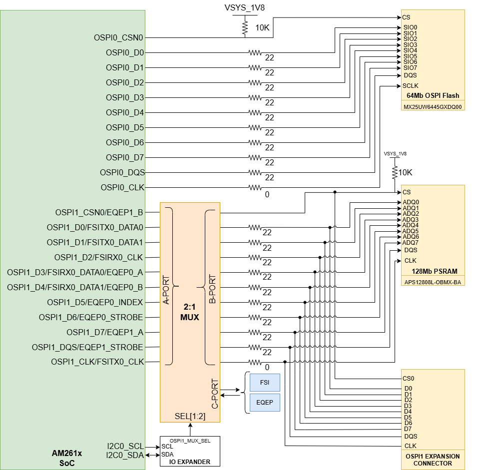
The pinout of the OSPI Expansion Connector can be found in Section 2.3.1, OSPI Expansion Connector.
LP-AM261 LP-AM261 OSPI Interface Figure 2-15 LP-AM261 OSPI Interface