SPRUJ06 October 2021
- Trademarks
- 1Introduction
- 2Revisions and Assembly Variants
- 3System Description
- 4Known Issues
3.3.1 Breakout Board Section
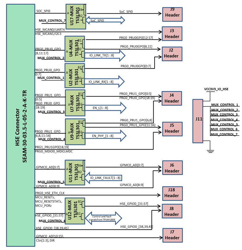
The general purpose Breakout board connects each pin of the High Speed Expansion (HSE) connector to eight, 2x10 test headers with 0.1” spacing between each pin. Additionally, the board features a circuit prototype area with standard 0.1” hole spacing.
Signals from the HSE connector are connected to the Breakout board or IO-Link section using FET switches. The FET switches are controlled using the J11 Header. Connecting the control signal of all the MUXes to ground routes all signals from the HSE connector to the Breakout board, whereas connecting the control signal to VCC3V3_IO_HSE routes all signals from the Mux to the IO-Link section.
Table 3-2 Functionality Selected by J11
Header
| J11 Header Selection | Functionality | Supported Board |
| Short J11 pins 1 and 2 | Selects IO-Link section | TMDS64DC01EVM only |
| Short J11 pins 2 and 3 | Selects Breakout board section | TMDS64DC01EVM and TMDS243DC01EVM |
 Figure 3-3 Breakout Sectional Functional Block
Diagram