SPRUIT0A December 2019 – May 2020
-
Jacinto7 EVM Infotainment Expansion
- Trademarks
- 1 Introduction
- 2 Infotainment Expansion Board Overview
- 3 Infotainment Expansion Board - User Setup/Configuration
- 4
Infotainment Expansion Board Hardware Architecture
- 4.1 Infotainment Expansion Board Hardware Top Level Diagram
- 4.2 Expansion Connectors
- 4.3 Board ID EEPROM
- 4.4 Audio Codec Interface
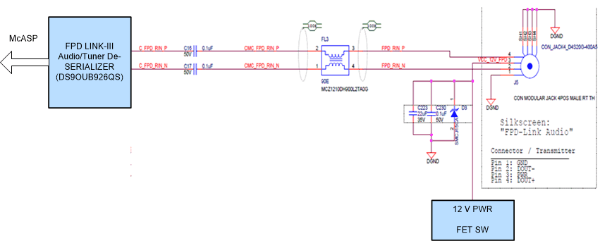
- 4.5 FPD link De-Serializer Interface (Audio)
- 4.6 DIR Interface
- 4.7 DIT Interface
- 4.8 Legacy Audio/JAMR3 Connectors
- 4.9 VIN/VOUT Mux Selection
- 4.10 HDMI Interface Bridge
- 4.11 FPD Link Display Serializer Interface
- 4.12 Parallel Camera Interface
- A Jacinto7 EVM Interface/IO Mapping
- Revision History
4.11 FPD Link Display Serializer Interface
FPD Link III serializer IC DS90UB921 is used for converting the 24 bit RGB signals Video signals from SOC into FPD link III signals. The serialized FPD link III output is terminated to HSD connector (Mfr Part# D4S20G-400A5-C). To route the VOUT signals from SOC to FPD link serializer from the default HDMI transmitter, see Table 10 and Section A.2.
I2C signals of J7 SOC being used for controlling and configuring the Display serializer. A 30.9 KΩ Pull up and 95.3K Ω pull down is provided on ID[X] pin to set the 7‘b I2C address to 0x1A.
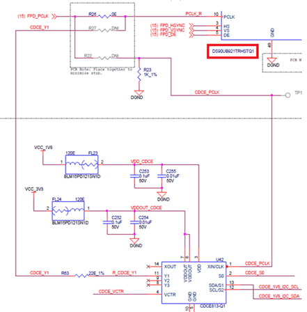
Power +12 V is provided to the HSD connector using a power switch TPS1H100AQPWPRQ1 to power the FPD Link-III display board. The power switch is controlled by a GPIO expander signal (PWR_SW_UB921). There is an optional clock cleaner circuit Mfr Part#:CDCE813-Q1 is available on infotainment board to clean the input clock signal coming from CP board and pass it to FPD link III Serializer.
 Figure 19. Optional Clock Cleaner to FPD Link Serializer
  Figure 20. FPD Link Display Serializer Interface