SNVAA33 December 2021 LM61460 , LM61460-Q1 , LM61495 , LM61495-Q1
3.1 Method 1: Feedback Resistor Switch Network
Figure 3-1 presents a simple approach to dynamically control the output voltage of a DC/DC step down buck converter through multiple parallel lower feedback resistors and switches. Controlling the switch will place the external lower resistors in parallel with RBOT to dynamically change the output voltage regulation point. Refer to Equation 1 for details on calculating the new output voltage. Though easy to implement, this control method has several drawbacks as listed below:
- Abrupt resistor switching to adjust VOUT from the lowest voltage to the highest voltage can cause the feedback node voltage to spike instantaneously and may trigger a false overvoltage protection (OVP) fault or PGOOD trigger low. The application design will need to be validated to ensure this does not occur.
- The component solution for multiple output voltages increase due to the additional lower feedback resistors and switches required to dynamically adjust VOUT. One way to minimize the switch components is to use a TS5A3359 (3:1, 1-channel analog multiplexer).
- For DC/DC step down buck converters utilizing a transconductance type error amplifier, the system is slightly difficult to properly compensate. This is because the lower feedback resistors directly impacts the gain of the system throughout the entire frequency range, which in turn impacts the crossover frequency of the system across different VOUT points and consequently affects the phase margin of the system. Refer to Figure 3-2 for the simulated LM61460-Q1 small signal loop response for the lowest output voltage of 5 V and the highest output voltage of 20 V. Note that the gain loop crosses 0 dB for at different crossover frequencies for different VOUT voltages and will have an impact on the system transient performance. Depending on the specific buck converter used, the output capacitance may need to be modified accordingly to create a stable design that is applicable across the entire VOUT voltage range.
 Figure 3-1 Feedback Resistor Switch
Network Control Scheme
Figure 3-1 Feedback Resistor Switch
Network Control Scheme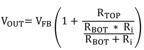
 Figure 3-2 Feedback Resistor Switch Network Control Scheme Bode Plot
For a TI USB Type-C dual buck reference design example using this feedback resistor switch network control method, refer to PMP22416.