SNVAA33 December 2021 LM61460 , LM61460-Q1 , LM61495 , LM61495-Q1
3.2 Method 2: Feedback Current Injection Network
This method controls the output voltage by an external current injection into the feedback node of the DC/DC buck converter as shown in Figure 3-3. In this control configuration, the system is:
- Easier to compensate since there is a fixed output voltage setpoint. The injected current lowers the voltage regulation point of the DC/DC buck converter from high to low.
- Smaller solution size since there is no need for additional bottom resistors to configure VOUT.
- The DC gain of the system loop remains constant throughout the entire typical USB Type-C VOUT range since the bottom resistor is set and fixed to a single component value. Refer to Figure 3-4 for the simulated LM61460-Q1 small signal loop response for the lowest output voltage of 5 V and the highest output voltage of 20 V using this control method. Note that the loop gain response crosses 0 dB at the same frequency for different VOUT voltages so the transient loop response is expected to be similar for all output voltage settings.
 Figure 3-3 Feedback Current Injection
Network Control Scheme
Figure 3-3 Feedback Current Injection
Network Control SchemeEquation 2. 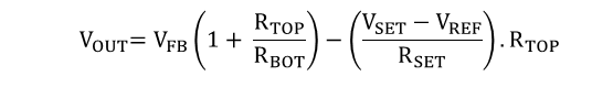
 Figure 3-4 Feedback Current Injection Network Control Scheme Bode Plot
For this application note, the current injection control method is used to demonstrate how the LM61460-Q1 and LM61495-Q1 design examples can be used in an USB Type-C applications. Refer to SLVA861 for additional reading material using the LM10011 current DAC as the external current injection source.
Design Procedure for Method 2
- Set the feedback network to regulate at the highest VOUT. For USB PD 3.0, the highest VOUT is 20 V. Note that setting the top and bottom resistors to output the highest VOUT enables a significantly reduced output capacitance solution that reduces overall solution size and solution cost.
- Set VSET equal to the feedback reference voltage for zero injection current at the highest VOUT setting. For the LM61460-Q1 and LM61495-Q1, VSET is set to 1 V since both DC/DC step down buck converter has an internal reference voltage (VREF) equal to 1 V.
- Calculate the required VSET for the desired output voltage regulation point from the equation shown in Equation 2.
- If a PWM signal followed by an RC filter is used to produce the DC bias voltage for the external injection current, it is important to have sufficient attenuation to remove unwanted ripple. It is recommended to have the corner frequency of RC filter at least two decade that of the PWM signal to get a 40 dB attenuation and prevent noise from coupling into the feedback node.