SLVUCG6 November 2022 TPS650350-Q1
- TPS650350-Q1 EVM User's Guide
- Trademarks
- 1 Introduction
- 2 Requirements
- 3 Operation Instructions
- 4 EVM Configurations
- 5 Test Points
- 6 Graphical User Interface
- 7 Typical Performance Plots
- 8 TPS650350-Q1 EVM Schematic
- 9 TPS650350-Q1 EVM PCB Layers
- 10TPS650350-Q1 EVM Bill of Materials
6.2.4.1 Using Device Configuration to Define Spin Settings
In some circumstances, TI may provide customized, pre-programmed devices for the camera application. Contact a local TI sales representative for more information.
The Device Configuration tabs in the GUI can be used to define custom settings for TI to pre-program into the device Non-Volatile Memory (NVM). Before beginning the spin definition, see the Camera PMIC Spin Selection Guide to determine if there is already a compatible spin for the target application, image sensor, or both.
Since the visual instruments in the Device Configuration page link directly to the corresponding bits and registers in the Register Map page, the Device Configuration page can be used to quickly define desired OTP register settings.
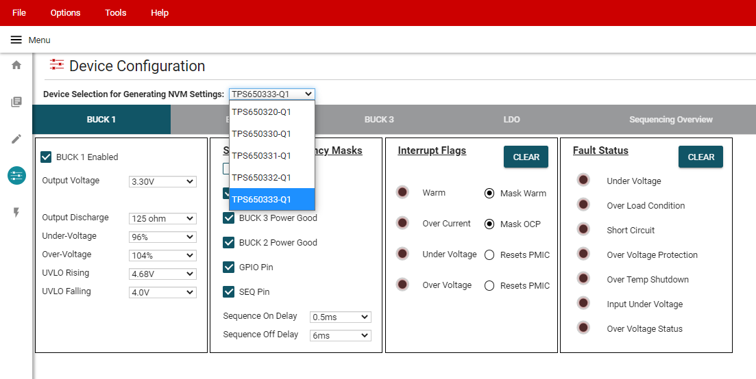
- Select the desired camera PMIC from the drop-down menu above the tab indicators to start. The GUI automatically shows, hides, or disables features corresponding to the selected PMIC. This drop down box is not adjustable if a device is connected to the GUI.
 Figure 6-8 Device Selection for Generating NVM Settings
Table 6-1 provides the equivalent device selection based on the GUI drop-down menu options
Table 6-1 Functionally Equivalent Generic Part NumbersGUI Option Functional Equivalent TPS650320-Q1 TPS650340-Q1 TPS650330-Q1 TPS650350-Q1 TPS650331-Q1 TPS650351-Q1 TPS650332-Q1 TPS650352-Q1 TPS650333-Q1 TPS650353-Q1 - Select the desired regulator, sequencing, and additional feature settings in each of the tabs. These changes are reflected in the Register Map page. For determining the power sequence settings, see Section 6.2.4.2.
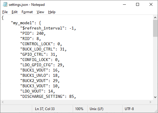
- Click File > Save Settings in the top left corner of the GUI to export the register settings in a JSON file. Provide the JSON file to TI to generate the NVM spin.
 Figure 6-9 Example Settings Output