SLVUCG6 November 2022 TPS650350-Q1
- TPS650350-Q1 EVM User's Guide
- Trademarks
- 1 Introduction
- 2 Requirements
- 3 Operation Instructions
- 4 EVM Configurations
- 5 Test Points
- 6 Graphical User Interface
- 7 Typical Performance Plots
- 8 TPS650350-Q1 EVM Schematic
- 9 TPS650350-Q1 EVM PCB Layers
- 10TPS650350-Q1 EVM Bill of Materials
6.3 In-Circuit Programming
The TPS650350-Q1 EVM demonstrates the in-circuit programming capabilities of the TPS650350-Q1 PMIC in a typical application. This section provides an example in-circuit programming procedure with application considerations.
- Verify the desired power, sequence, and other settings using the GUI's Sequencing Overview tools. See Configuring the Power Sequence.
- Once settings are verified and validated, configure the TPS650350-Q1 EVM for a typical camera application:
- Ensure the I2C pull-up jumper is populated at J6.
- Supply the PMIC VIO with either the Buck 1 or Buck 2 output. See Selecting the Logic Supply Voltage.
- Tie the PMIC VSYS/PVIN_B1 input voltage to VIN. See Buck 1 Input Supply.
- Supply the PMIC Buck 2, Buck 3, and LDO with the Buck 1 output. See Selecting Regulator Input Supplies.
- Assert SEQ (S1) before applying power.
- Apply a Buck 1 input voltage (typical is 12 V) to power up the device. By default, the Buck 1 and Buck 2 regulators are enabled, allowing the 3.3 V and 1.8 V rails to power up.
- In a typical camera application, this may be sufficient to power up the serializer and enable PMIC programming over the Serializer-Deserializer (SerDes) back-channel.
- If additional rails are required, assert GPIO (S4) to enable the Buck 3 and LDO regulators.
- Unlock the configuration and control registers.
- Re-program the PMIC settings. If changing a regulator output voltage, TI recommends disabling the regulator first. If doing this in an application setting shuts down a critical component, change the output voltage in small steps to prevent triggering under or over-voltage fault handling.
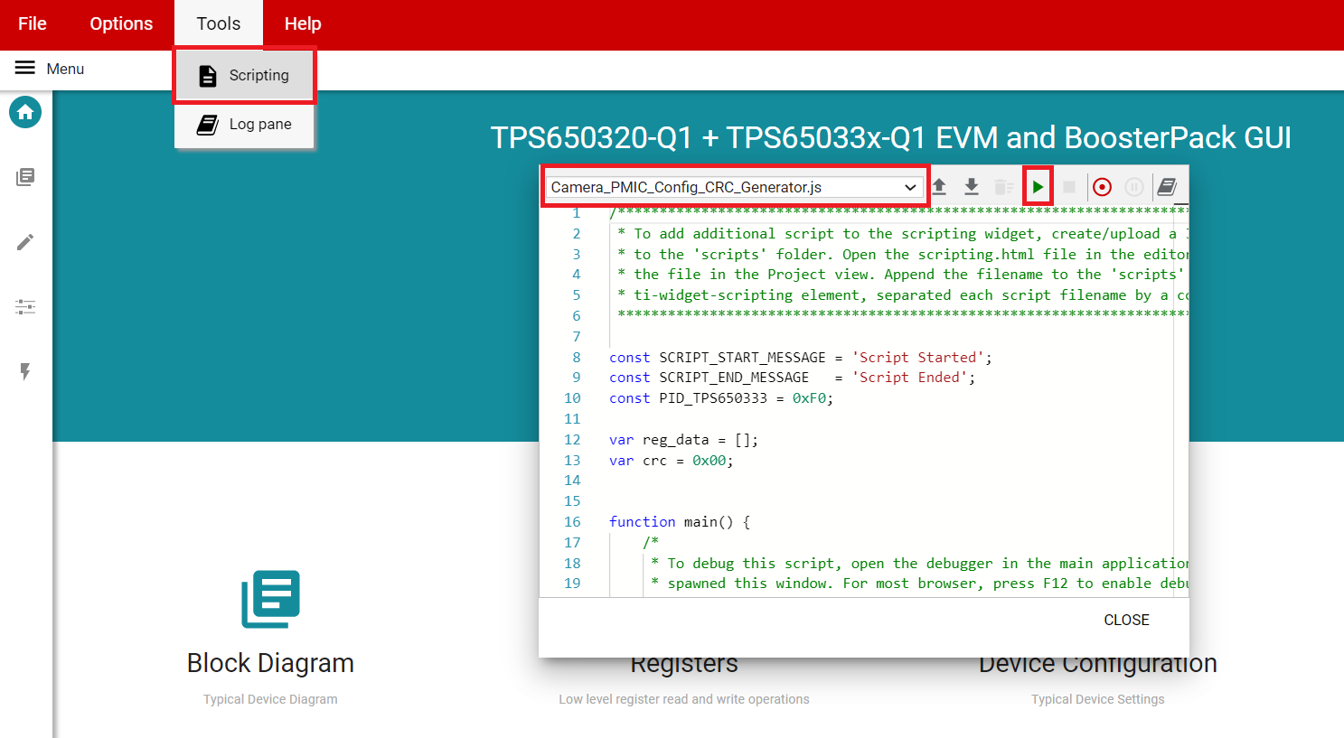
- If the device configuration Cyclic Redundancy Check (CRC) is enabled, calculate and write the new configuration CRC by running the GUI's built-in script. For more information on the GUI's capabilities for programming automation, see the BOOSTXL-TPS65033 User's Guide.
 Figure 6-14 GUI Configuration CRC Script
 - Burn the final PMIC register settings to EEPROM.
- Validate the settings on subsequent startups.