SLVUBZ0A November 2020 – December 2020
5 PCB Layout
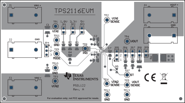
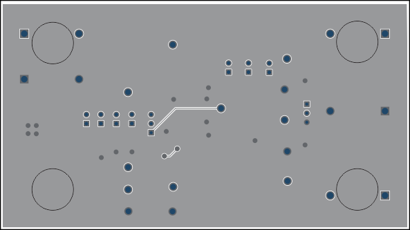
Figure 5-1 and Figure 5-2 show the TPS2116EVM PCB layout images.
 Figure 5-1 TPS2116 Top Layer
 Figure 5-2 TPS2116 Bottom Layer
SLVUBZ0A November 2020 – December 2020
Figure 5-1 and Figure 5-2 show the TPS2116EVM PCB layout images.
 Figure 5-1 TPS2116 Top Layer
 Figure 5-2 TPS2116 Bottom Layer