SLVU281B May 2009 – August 2021
2.9 Powering Up
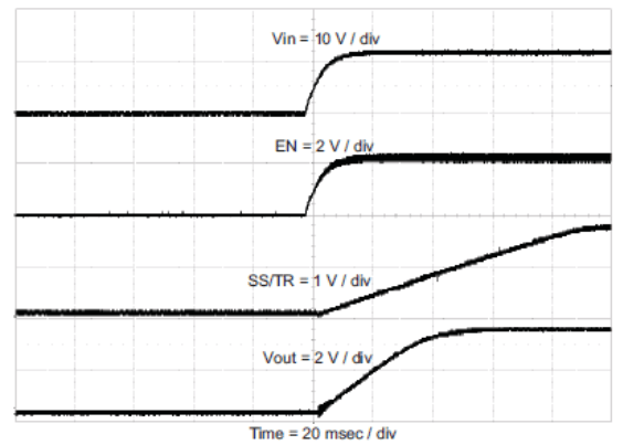
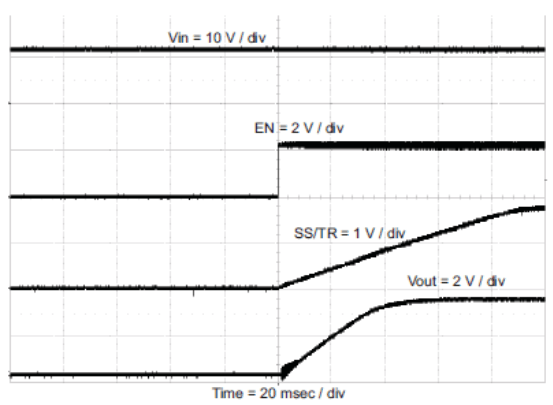
Figure 2-9 and Figure 2-10 show the start-up waveforms for the TPS54620EVM-374 . In Figure 2-9, the output voltage ramps up as soon as the input voltage reaches the UVLO threshold as set by the R1 and R2 resistor divider network. In Figure 2-10, the input voltage is initially applied and the output is inhibited by using a jumper at J2 to tie EN to GND. When the jumper is removed, EN is released. When the EN voltage reaches the enable-threshold voltage, the start-up sequence begins and the output voltage ramps up to the externally set value of 3.3 V. The input voltage for these plots is 12 V and the load is 1Ω.
 Figure 2-9 TPS54620EVM-374 Start-Up Relative to VIN
 Figure 2-10 TPS54620EVM-374 Start-up Relative to Enable