SLVU157A March 2006 – October 2021
3.1 Layout
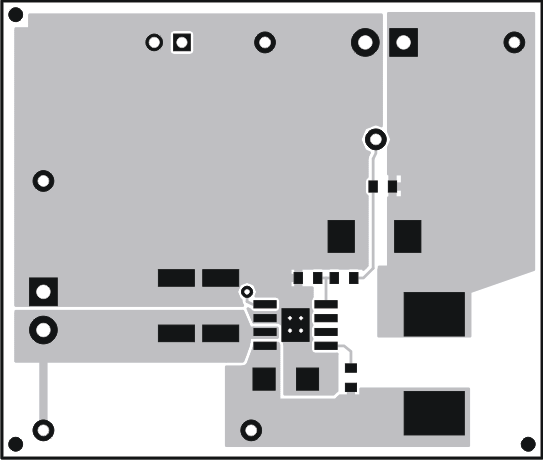
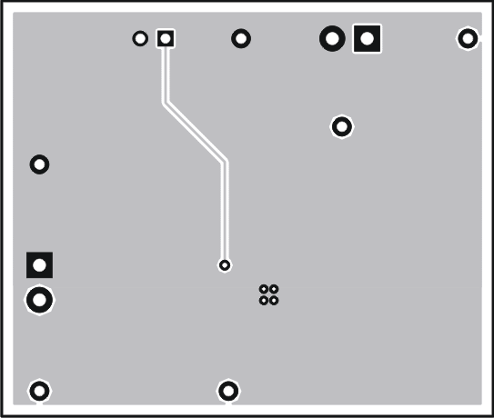
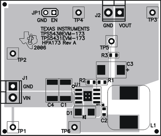
The board layout for the TPS5430EVM-173 and TPS5431EVM-173 is shown in Figure 3-1 through Figure 3-3. Both EVM circuits use the same printed-circuit board (HPA173). The topside layer of the EVM is laid out in a manner typical of a user application. The top and bottom layers are 2-oz. copper.
The top layer contains the main power traces for VIN, OUT, and VPHASE. Also on the top layer are connections for the remaining pins of the TPS5430 and a large area filled with ground. The bottom layer contains ground and signal routes for the ENA feature. The top and bottom and internal ground traces are connected with multiple vias placed around the board including four vias directly under the TPS5430 device to provide a thermal path from the PowerPAD™ land to ground.
The input decoupling capacitor (C1) and bootstrap capacitor (C2) are all located as close to the IC as possible. In addition, the voltage set-point resistor divider components are also kept close to the IC. The voltage divider network ties to the output voltage at the point of regulation, the copper Vout trace past the output capacitor C3. For the TPS5430, an additional input bypass capacitor (C4) is required.
 Figure 3-1 Top-Side Layout
 Figure 3-2 Bottom-Side Layout (Looking From Top Side)
 Figure 3-3 Top-Side Assembly