SLVAF84 September 2021 DRV8311 , DRV8312 , DRV8313 , DRV8316 , MCT8316Z
5 Delay Compensation to Minimize Duty Cycle Distortion
Differences in delays in dead time and propagation delay can cause mismatches in output timings of PWMs, which can lead to duty cycle distortion. To accommodate differences in propagation delay between the conditions mentioned previously in this application note, some devices in the DRV831x and MCx831x families integrate a Delay Compensation feature.
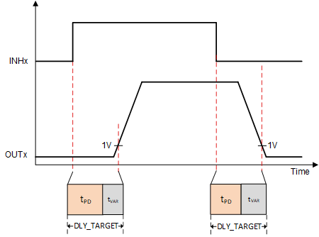
 Figure 5-1 Delay Compensation With Current Flowing Out of the Phase
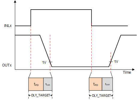
 Figure 5-2 Delay Compensation With Current Flowing Into the Phase
Delay Compensation is used to match delay times for currents going into and out of phase by adding variable delay time (tvar) to match a preset target delay time. This delay time is configurable in SPI devices, and it is recommended in the data sheets to choose a target delay time that is equal to the propagation delay time plus driver dead time (tpd + tdead).
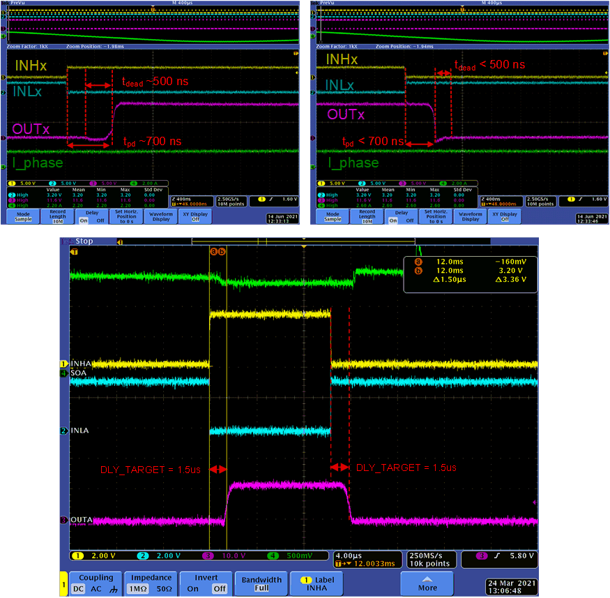
In the following example, observe that the DRV8316 again uses a fixed slew rate of 200 V/μs and synchronous PWM inputs. Compare the propagation delays of Figure 5-3 without and with Delay Compensation.
 Figure 5-3 Comparison of DRV8316 Output Waveforms With and Without 1.5 μs of Delay Compensation
In the top two waveforms in Figure 5-3, Delay Compensation is disabled and results in a mismatch of propagation delays and dead time due to the direction of the current at the OUTx pin, causing output duty cycle distortion.
In the bottom waveform in Figure 5-3, Delay Compensation is enabled and the delay target time is set to DLY_TARGET = 1.5 μs, resulting in matching propagation delays and a reduction of output duty-cycle distortion.